Semiconductor circuit, display device, electronic apparatus

a technology of semiconductors and circuits, applied in logic circuit coupling/interface arrangements, pulse techniques, instruments, etc., can solve the problems of reduced yield, increased layout area, and reduced yield, so as to reduce layout area, reduce variation in performance, and improve yield

Active Publication Date: 2006-09-28
SEMICON ENERGY LAB CO LTD
View PDF17 Cites 12 Cited by
  • Summary
  • Abstract
  • Description
  • Claims
  • Application Information

AI Technical Summary

Benefits of technology

[0014] In order to solve the aforementioned problems, the invention provides a semiconductor circuit where the number of transistors can be reduced by using n-channel transistors and p-channel transistors instead of using the 2 clocked inverters that have a total of 8 transistors and thus occupy the semiconductor circuit in FIGS. 23 and 24.
[0023] In addition, the invention can provide a display device where the number of transistors can be reduced by using n-channel transistors and p-channel transistors instead of using 2 clocked inverters that have a total of 8 transistors and thus occupy the semiconductor circuit in FIGS. 23 and 24.
[0031] In addition, the invention can provide an electronic appliance where the number of transistors can be reduced by using n-channel transistors and p-channel transistors instead of using 2 clocked inverters that have a total of 8 transistors and thus occupy the semiconductor circuit in FIGS. 23 and 24.
[0038] In accordance with the invention, the number of transistors that constitute a semiconductor circuit can be reduced from 10 to 6, thereby the layout area can be reduced. In particular, the semiconductor circuit of the invention can be particularly effectively applied to the case of using multiple stages of semiconductor circuits such as a shift register circuit or a latch circuit, thereby variations in performance can be suppressed in manufacturing transistors, and also the yield can be expected to be improved.
[0039] In the display device using the semiconductor circuit of the invention, by reducing the number of transistors that constitute the semiconductor circuit from 10 to 6, the layout area of a peripheral circuit can be reduced in accordance with the increased area of the pixel portion. In the case of integrally forming transistors of a pixel portion and a peripheral circuit over a common substrate, the number of transistors that constitute the semiconductor circuit can be reduced from 10 to 6 by applying the semiconductor circuit of the invention, thereby variations in performance of transistors can be suppressed, and also the yield can be expected to be improved the yield can be expected to be improved.
[0040] In the electronic apparatus using the semiconductor circuit of the invention, the layout area of a display portion can be reduced; therefore, the electronic apparatus can be reduced in size and weight. Further, products with a high yield can be manufactured, so that products can be provided to customers at lower cost.

Problems solved by technology

In addition, such a problem is posed that the yield is decreased resulting from variations of transistors in accordance with the increased number of transistors for constructing the circuit.
As set forth above, a semiconductor circuit that constitutes a shift register circuit or a latch circuit has problems presently on the configuration such as an increased layout area and a decreased yield.

Method used


Image

  • Semiconductor circuit, display device, electronic apparatus
  • Semiconductor circuit, display device, electronic apparatus
  • Semiconductor circuit, display device, electronic apparatus

Examples


embodiment mode 1

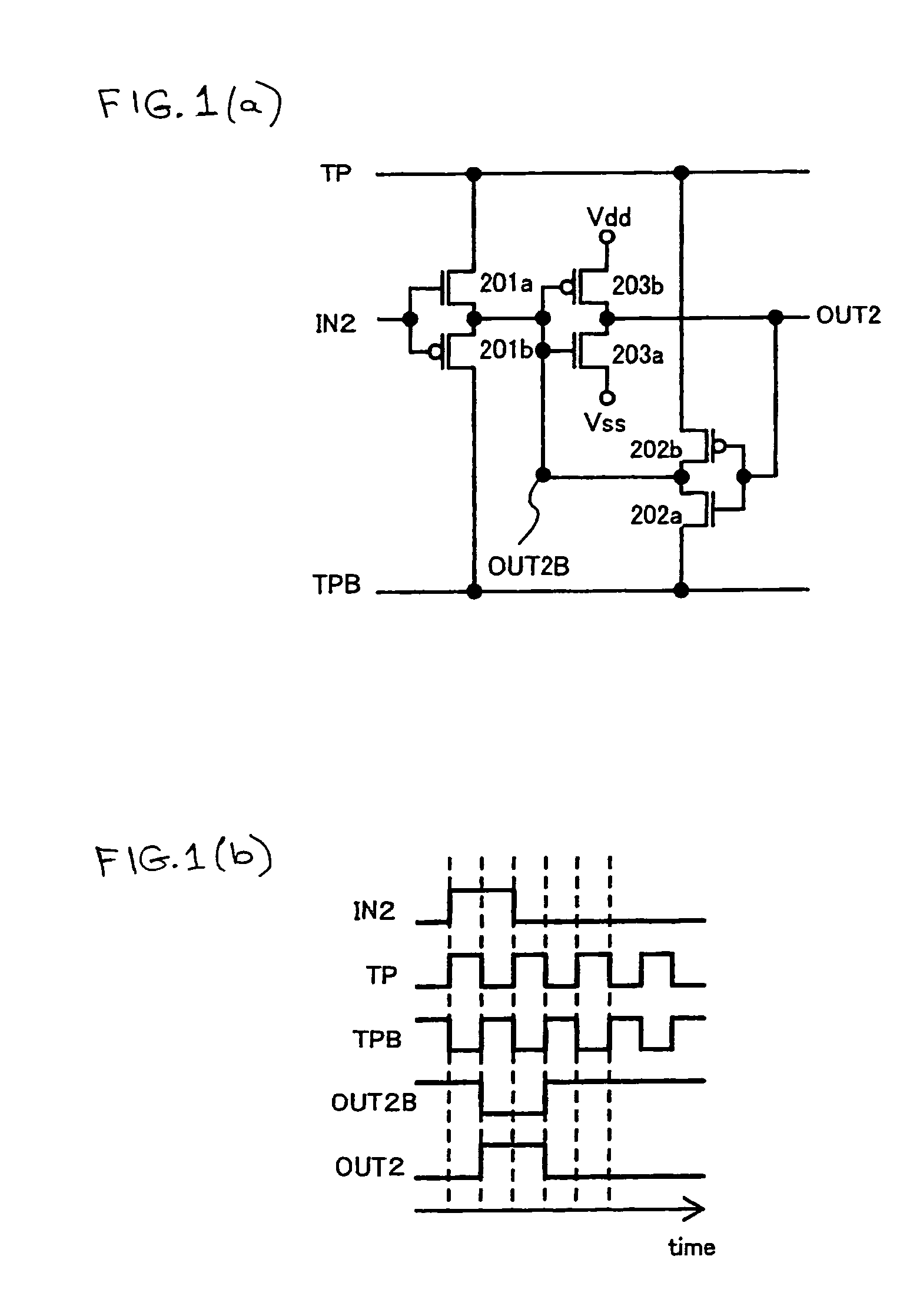
[0065]FIG. 1(a) shows one embodiment mode of a semiconductor circuit of the invention. As shown in FIG. 1(a), the first clocked inverter CKINV1 and the second clocked inverter CKINV2 of a conventional semiconductor circuit are replaced by circuits constructed of n-channel transistors and p-channel transistors. Here, the n-channel transistors and the p-channel transistors correspond to a first n-channel transistor 201a, a first p-channel transistor 201b, a second n-channel transistor 202a, and a second p-channel transistor 202b. In this specification, a terminal to serve as a source electrode or a drain electrode of the first n-channel transistor 201a, and a terminal to serve as a source electrode or a drain electrode of the second p-channel transistor 202b, to each of which a timing control signal TP is inputted, are called first terminals. In addition, a terminal to serve as a source electrode or a drain electrode of the first p-channel transistor 201b, and a terminal to serve as a...

embodiment 1

[0083] Description is made below on an embodiment of the invention.

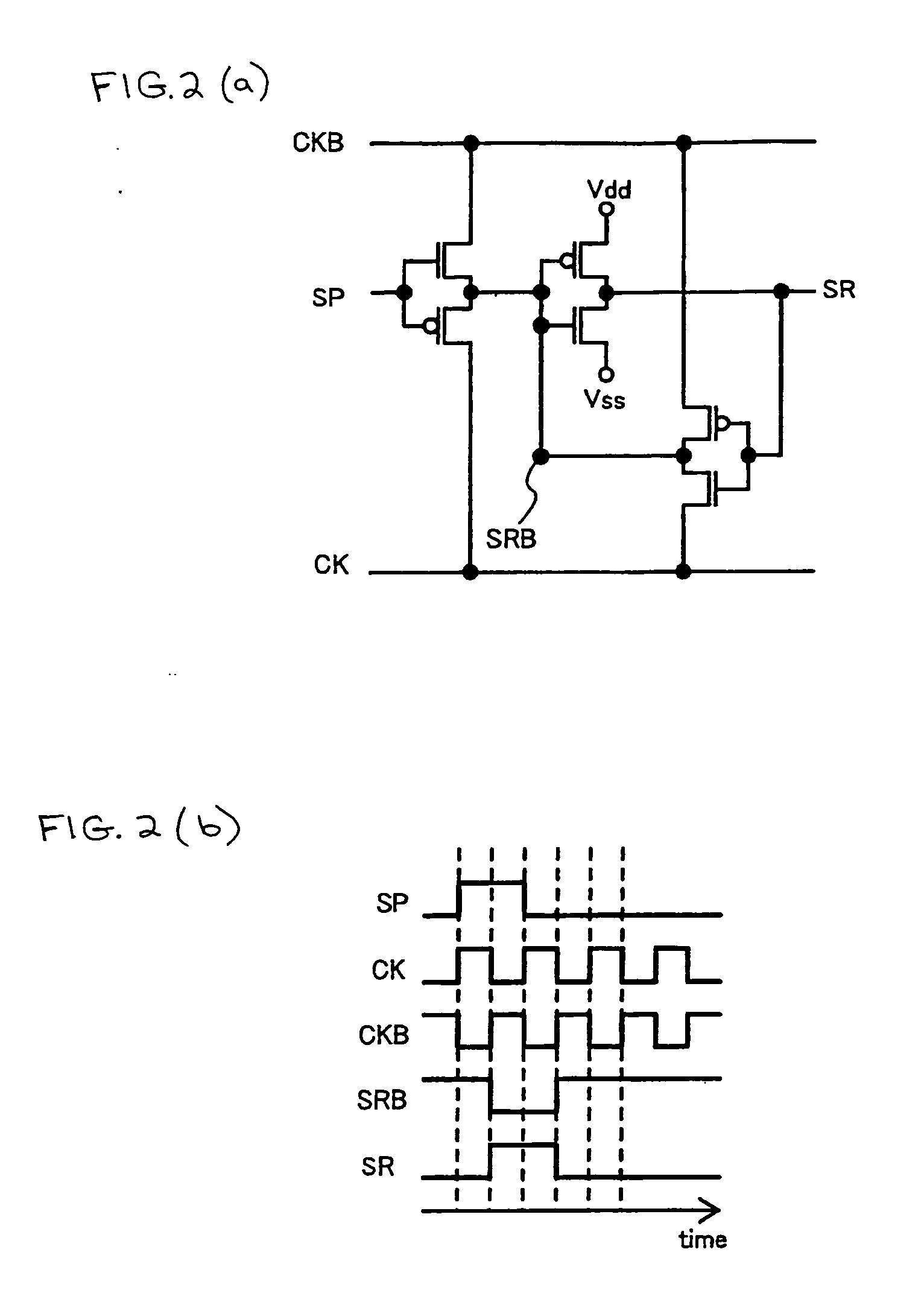
[0084]FIG. 2(a) is a circuit constructed for the purpose of using the semiconductor circuit of the invention as a shift register circuit. Here, a start pulse SP is used as the input signal IN, a clock signal CK is used as the timing control signal TP, and an inverted clock signal CKB is used as the inverted timing control signal TPB. In addition, the circuit outputs SR.

[0085]FIG. 2(b) shows a timing chart of FIG. 2(a). Description on the operation of the timing chart in FIG. 2(b) is omitted since it is shown in Embodiment Mode 1.

[0086]FIG. 3(a) shows an example where four stages of the shift register circuit in FIG. 2(a) are used. FIG. 3(b) shows a timing chart thereof. Note that an output of a first-stage shift register is SR1, an output of a second-stage shift register is SR2, an output of a third-stage shift register is SR3, and an output of a fourth-stage shift register is SR4.

[0087] In constructing multiple ...

embodiment 2

[0091]FIG. 5(a) is a circuit constructed for the purpose of using the semiconductor circuit of the invention as a latch circuit. Here, a data signal DATA is used as the input signal IN, a sampling pulse LSP is used as the timing control signal TP, and an inverted sampling pulse LSPB is used as the inverted timing control signal TPB. In addition, the circuit outputs D_OUT.

[0092] FIGS. 5(b), (c), (d) and (e) show timing charts of FIG. 5(a). Note that an initial state of the output D_OUT is at “Lo”. As for the operation of the timing charts in FIGS. 5(b), (c), (d) and (e), the data signal DATA is sampled when the sampling pulse LSP is at “Lo” whereas the previous output is held when the sampling pulse LSP is at “Hi” as shown in Embodiment Mode 1. In each of the timing charts, it can be seen that the data signal DATA right before the sampling pulse LSP changes from “Lo” to “Hi” continues to be held.

[0093]FIG. 6(a) is a diagram showing an example of actually designing the latch circuit...


PUM


Abstract

To provide a semiconductor circuit having D flip-flops, a display device and an electronic apparatus having the display device, in the invention, the number of transistors is reduced by using 2 n-channel transistors and 2 p-channel transistors instead of using 2 conventional clocked inverters that have a total of 8 transistors in D flip-flops.

Description

FIELD OF THE INVENTION [0001] The present invention relates to a semiconductor circuit. In particular, the invention relates to a semiconductor circuit configured with transistors. In addition, the invention relates to a display device having the semiconductor circuit, and an electronic apparatus having the display device. [0002] Note that the semiconductor circuit herein means all circuits that can function by utilizing the semiconductor characteristics. BACKGROUND OF THE INVENTION [0003] As a driver circuit of a display device, a semiconductor circuit that is inputted with signals for controlling the operation timing of transistors is used for various semiconductor devices. [0004] Note that the semiconductor device in this specification means all devices that can function by utilizing the semiconductor characteristics, and all of electronic optical devices and electronic apparatuses fall within the category of the semiconductor device. [0005]FIG. 23 shows a configuration example o...

Claims


Application Information

Patent Timeline
Patent Type & Authority Applications(United States)
IPC IPC(8): G09G3/36
CPCG09G3/3266G09G3/3291G09G3/3677G09G3/3688G09G2310/0286G09G2310/0294G11C19/00G11C19/28
Inventor NAGATSUKA, SHUHEI
Owner SEMICON ENERGY LAB CO LTD
Why Eureka
Try Eureka