
Methods of forming trench isolation in the fabrication of integrated circuitry and methods of fabricating integrated circuitry

a technology of integrated circuitry and trench isolation, which is applied in the direction of basic electric elements, semiconductor/solid-state device manufacturing, electric apparatus, etc., can solve the problems of unsatisfactory void formation within the trenches, added time required to remove such materials, and silicon dioxide deposition which is not as dense as desired

Active Publication Date: 2006-09-28
MICRON TECH INC
View PDF5 Cites 19 Cited by
  • Summary
  • Abstract
  • Description
  • Claims
  • Application Information

AI Technical Summary

Benefits of technology

The invention provides methods for making integrated circuitry with trench isolation. The methods involve depositing a spin-on-dielectric over a semiconductor substrate, etching some of the dielectric, and annealing the remaining dielectric to form a different composition. This results in a more effective isolation of the semiconductor material. The methods also involve forming narrow and wider isolation trenches and depositing the dielectric accordingly to achieve better results. Overall, the methods improve the performance and reliability of integrated circuitry.

Problems solved by technology

Yet as trenches have become deeper and narrower, high density plasma deposited oxides can result in undesired void formation within the trenches during filling.
Such latter processes, while resulting in good void-free gap filling, typically result in a silicon dioxide deposition which is not as dense as desired.
This of course adds to the time required to later remove such material from laterally outward of the trenches.
Further even with spin-on-dielectrics, it is sometimes very difficult to get the material deep within high aspect ratio trenches to densify at the bases of such trenches.

Method used


Image

  • Methods of forming trench isolation in the fabrication of integrated circuitry and methods of fabricating integrated circuitry
  • Methods of forming trench isolation in the fabrication of integrated circuitry and methods of fabricating integrated circuitry
  • Methods of forming trench isolation in the fabrication of integrated circuitry and methods of fabricating integrated circuitry

Examples


Embodiment Construction

[0018] This disclosure of the invention is submitted in furtherance of the constitutional purposes of the U.S. Patent Laws “to promote the progress of science and useful arts” (Article 1, Section 8).

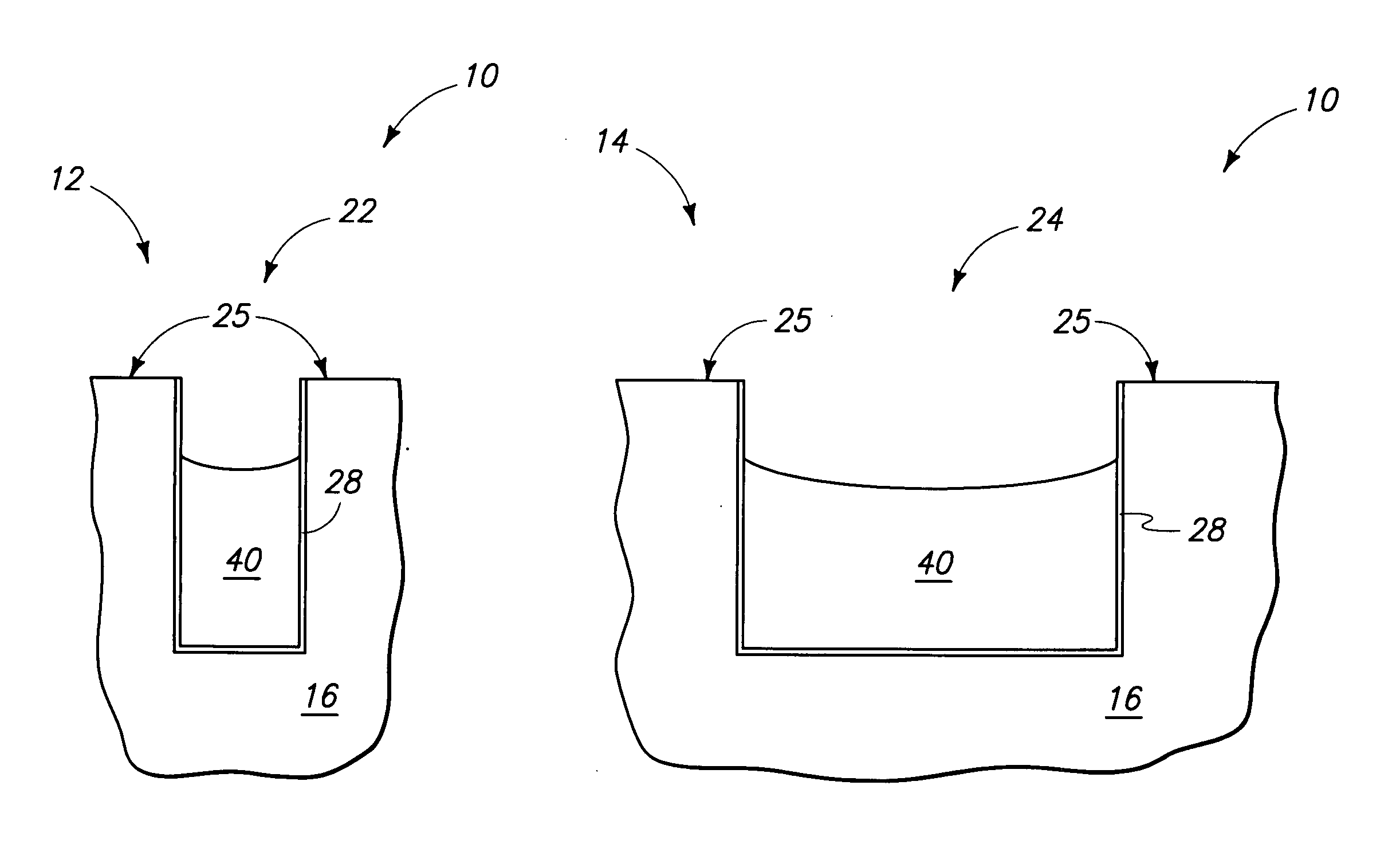
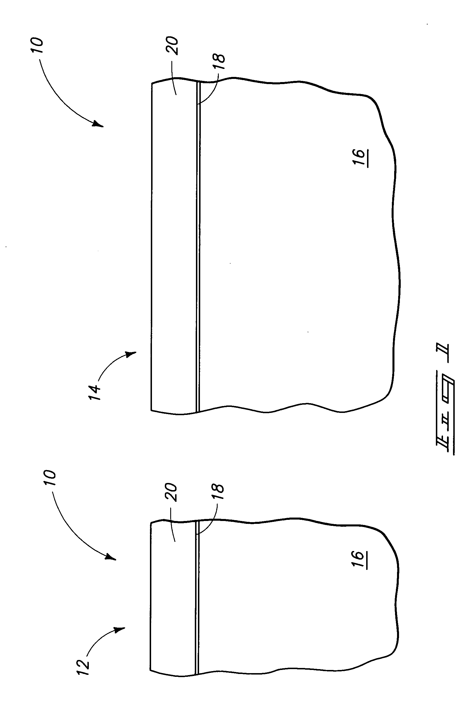
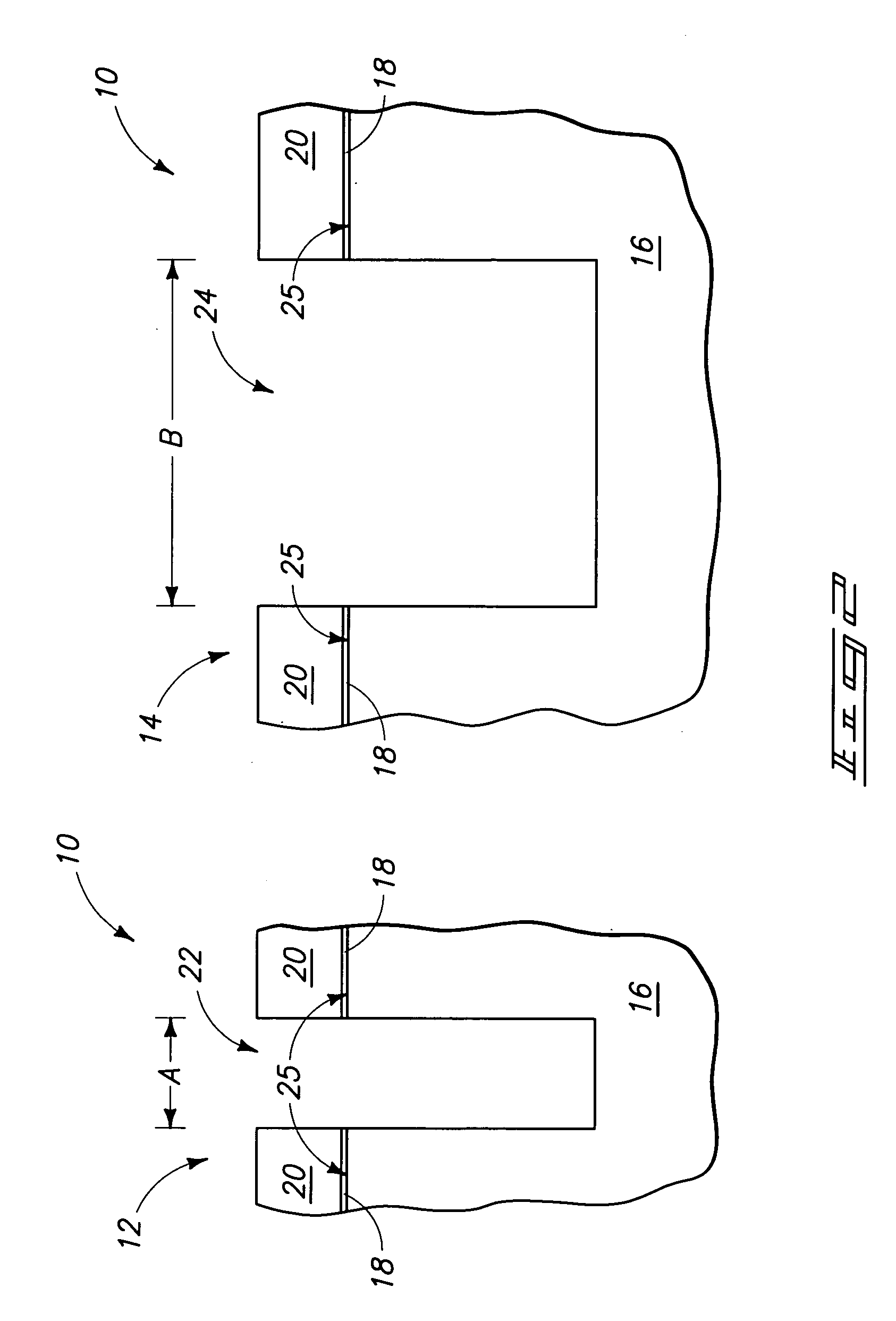
[0019] The invention contemplates methods of forming trench isolation in the fabrication of integrated circuitry, and to methods of fabricating integrated circuitry independent of whether trench isolation is fabricated. Referring initially to FIG. 1, a semiconductor substrate in process is indicated generally with reference numeral 10. In the context of this document, the term “semiconductor substrate” or “semiconductive substrate” is defined to mean any construction comprising semiconductive material, including, but not limited to, bulk semiconductive materials such as a semiconductive wafer (either alone or in assemblies comprising other materials thereon), and semiconductive material layers (either alone or in assemblies comprising other materials). The term “substrate“refers to any ...


PUM

PropertyMeasurementUnit
temperatureaaaaaaaaaa

Abstract

A method of fabricating integrated circuitry includes depositing a spin-on-dielectric over a semiconductor substrate. The spin-on-dielectric comprises a polysilazane. Only some of the polysilazane is etched from the semiconductor substrate. Such etching comprises exposure to an etching fluid comprising at least one of a) an aqueous fluid having a pH greater than 7.0, or b) a basic fluid solution. After the etching, remaining spin-on-dielectric comprising polysilazane is annealed effective to form an annealed dielectric which is different in composition from the spin-on-dielectric, and preferably having a dielectric constant k which is different from that of the initially deposited spin-on-dielectric.

Description

TECHNICAL FIELD [0001] This invention relates to methods of forming trench isolation in the fabrication of integrated circuitry and to methods of fabricating integrated circuitry. BACKGROUND OF THE INVENTION [0002] In the fabrication of integrated circuitry, numerous devices are packed onto a single small area of a semiconductor substrate to create an integrated circuit. Many of the individual devices are electrically isolated from one another. Accordingly, electrical isolation is an integral part of semiconductor device design for preventing unwanted electrical coupling between adjacent components and devices. [0003] As the size of integrated circuits is reduced, the devices that make up the circuits are positioned closer together. Conventional methods of isolating circuit components use trench isolation. Such is typically formed by etching trenches into a semiconductor substrate and filling the trenches with insulative material. As the density of components on the semiconductor su...

Claims


Application Information

Patent Timeline
Patent Type & Authority Applications(United States)
IPC IPC(8): H01L21/76
CPCH01L21/02164H01L21/02222H01L21/02238H01L21/02255H01L21/02282H01L21/02337H01L21/31055H01L21/31133H01L21/3125H01L21/76229
Inventor SMYTHE, JOHNLI, LIFUCSKO, JANOS
Owner MICRON TECH INC
Learn More