Magnetoresistive effect element and method for fabricating the same

Inactive Publication Date: 2006-10-05
FUJITSU LTD
View PDF1 Cites 56 Cited by
  • Summary
  • Abstract
  • Description
  • Claims
  • Application Information

AI Technical Summary

Benefits of technology

[0010] In the conventional magnetoresistive effect element shown in FIG. 10B, the edge of the pinned magnetic layer 104 is spaced from the edge of the free magnetic layer 108, whereby the influences of the leakage magnetic field from the pinned magnetic layer 104 and the staying-back objects can be decreased. However, the large area of the pinned magnetic layer 104 is unsuitable for high integration. When the pinned magnetic layer 104 is made smaller, due to the disalignment of the free magnetic layer 108 with the pinned magnetic layer 104, the influence of the leakage magnetic field from the pinned magnetic layer 104 is changed, which often causes erroneous writing and erroneous reading.
[0011] An object of the present invention is to provide a magnetoresistive effect element which can suppress erroneous writing and erroneous reading due to the fluctuation of the leakage magnetic field from the pinned magnetic layer, and a method for fabricating the magnetoresistive effect element. Another object of the present invention is to provide a magnetic memory device of high reliability, which comprises the magnetoresistive effect element.
[0012] According to one aspect of the present invention, there is provided a magnetoresistive effect element comprising: a first ferromagnetic layer; a nonmagnetic layer formed on the first ferromagnetic layer; a second ferromagnetic layer formed on the nonmagnetic layer; and a sidewall insulating film formed on a side wall of the second ferromagnetic layer, an end of the first ferromagnetic layer being aligned with an end of the sidewall insulating film.
[0013] According to another aspect of the present invention, there is provided a method for fabricating a magnetoresistive effect element comprising the steps of: forming a first ferromagnetic layer; forming a nonmagnetic layer on the first ferromagnetic layer; forming a second ferromagnetic layer on the nonmagnetic layer; forming a cap layer of a nonmagnetic material on the second ferromagnetic layer; patterning the cap layer and the second ferromagnetic layer in

Problems solved by technology

Resultantly, the magnetic field (Hfc) which changes the resistance state is shifted to often cause erroneous writin

Method used


Image

  • Magnetoresistive effect element and method for fabricating the same
  • Magnetoresistive effect element and method for fabricating the same
  • Magnetoresistive effect element and method for fabricating the same

Examples


Example

[0020] The magnetic memory device and the method for fabricating the same according to one embodiment of the present invention will be explained with reference to FIGS. 1 to 9B.

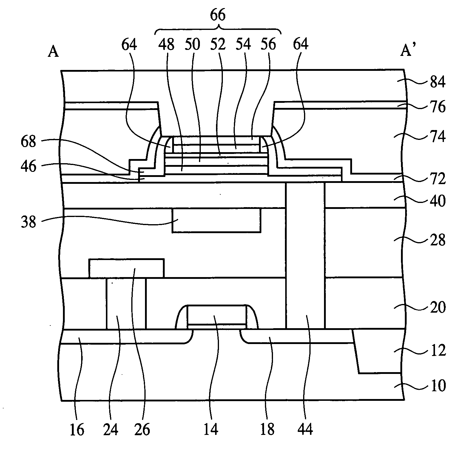
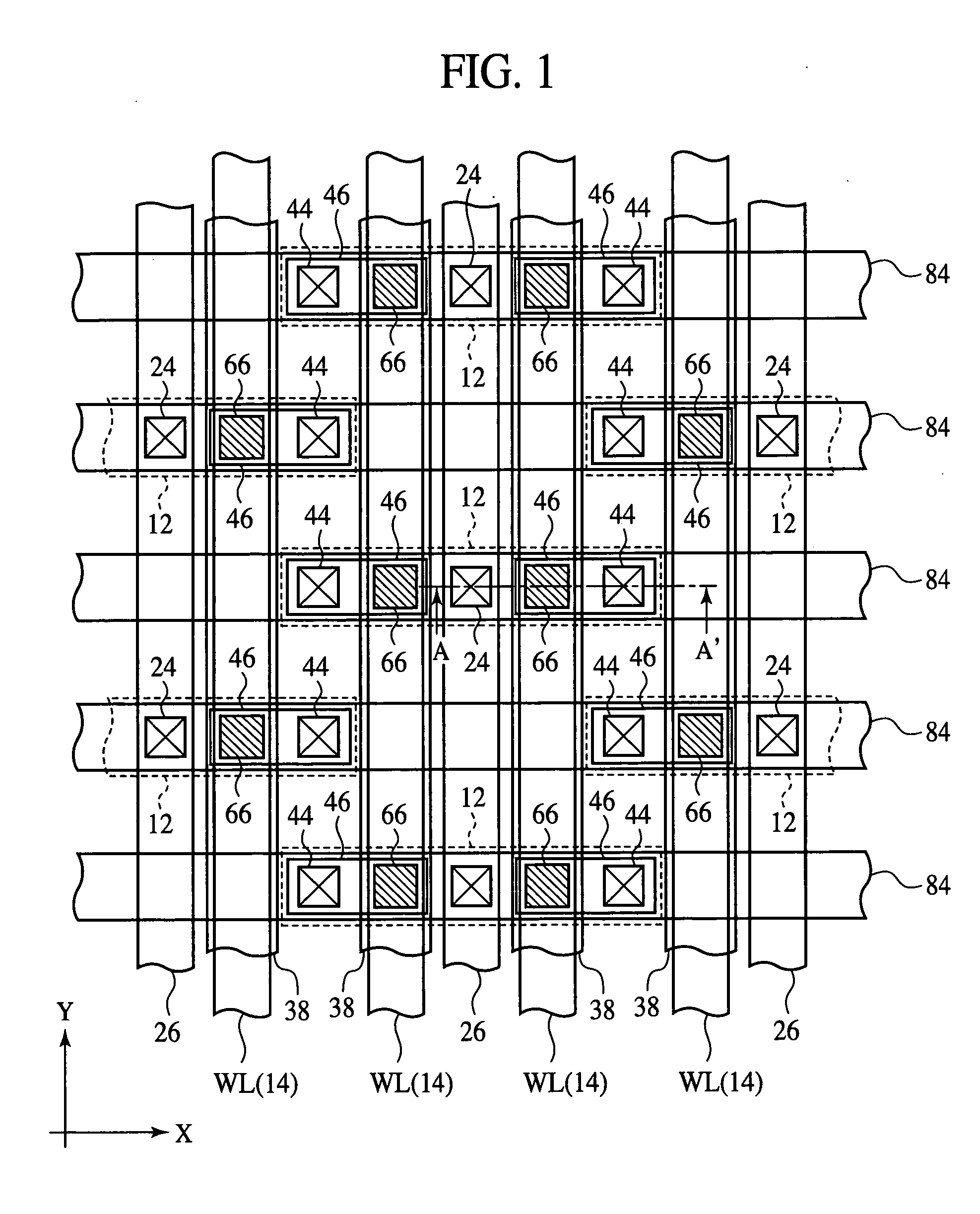
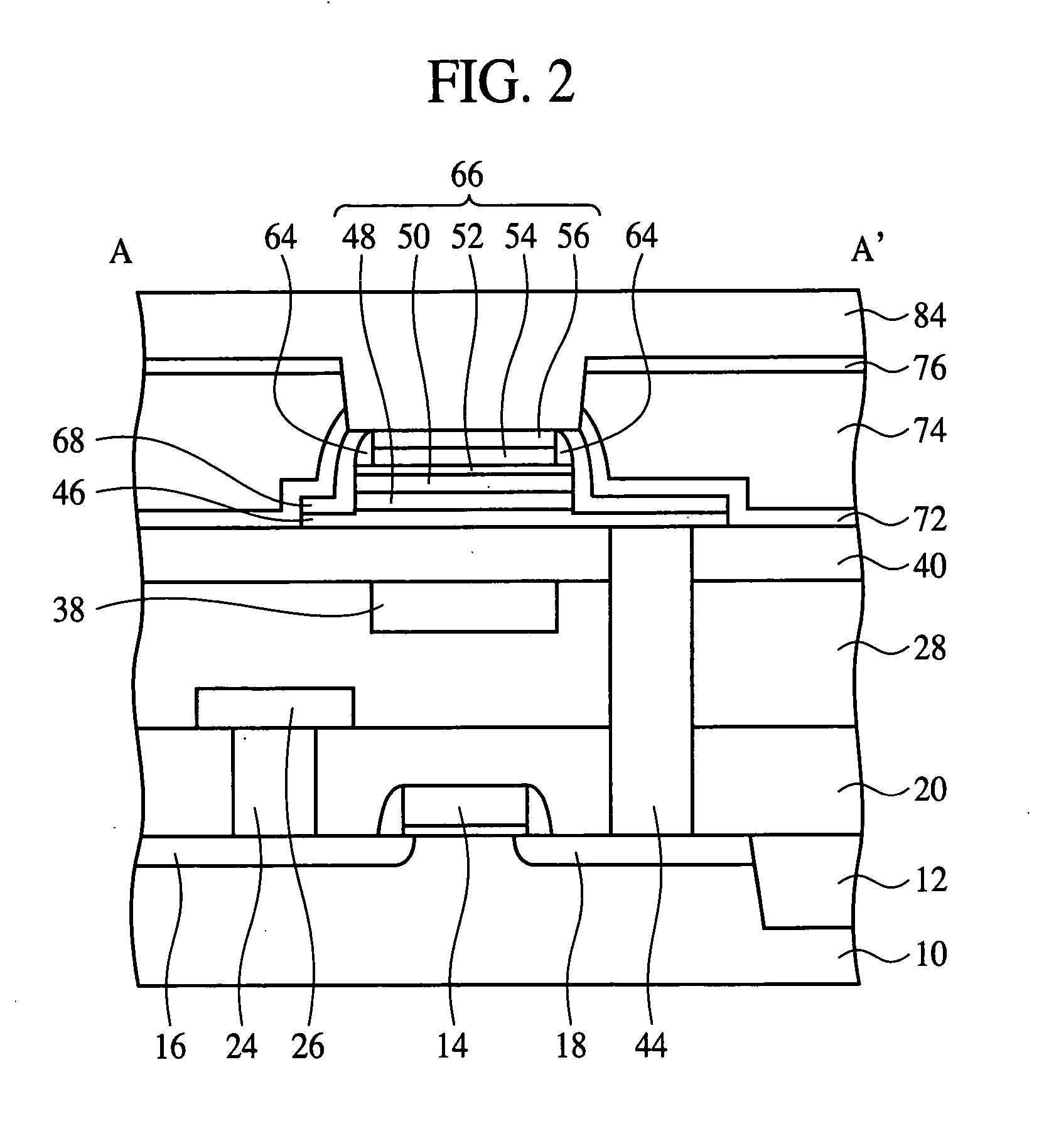
[0021]FIG. 1 is a plan view showing the structure of the magnetic memory device according to the present embodiment. FIG. 2 is a diagrammatic sectional view showing the structure of the magnetic memory device according to the present embodiment. FIGS. 3A to 9B are sectional views showing the method for fabricating the magnetic memory device according to the present embodiment.

[0022] First, the structure of the magnetic memory device according to the present embodiment will be explained with reference to FIGS. 1 and 2. FIG. 2 is the sectional view along the line A-A′ in FIG. 1.

[0023] A device isolation film 12 for defining a plurality of active regions is formed on a silicon substrate 10. The respective active regions have a rectangular shape which is elongated in the X-direction and are arranged in zigzag....


PUM


Abstract

The magnetoresistive effect element comprises a first ferromagnetic layer 50, a nonmagnetic layer 52 formed on the first ferromagnetic layer 50, a second ferromagnetic layer 54 formed on the nonmagnetic layer 52, and a sidewall insulating film 64 formed on the side wall of the second ferromagnetic layer 54. The end of the first ferromagnetic layer 50 is aligned with the end of the sidewall insulating film 64. Whereby the disalignment between the first ferromagnetic layer and the second ferromagnetic layer can be prevented.

Description

CROSS-REFERENCE TO RELATED APPLICATIONS [0001] This application is based upon and claims the benefit of priority from the prior Japanese Patent Application No. 2005-080311, filed on Mar. 18, 2005, the entire contents of which are incorporated herein by reference. BACKGROUND OF THE INVENTION [0002] The present invention relates to a magnetoresistive effect element, more specifically, a magnetoresistive effect element whose resistance value is varied depending on magnetization directions of the magnetic layers, and a method for fabricating the magnetoresistive effect element. [0003] Recently, as a rewritable nonvolatile memory, a magnetic random access memory (hereinafter called an MRAM) including magnetoresistive effect elements arranged in a matrix is noted. The MRAM memorizes information by using combinations of magnetization directions of two magnetic layers and reads memorized information by detecting resistance changes (i.e., current changes or voltage changes) between when magn...

Claims


Application Information

Patent Timeline
IPC IPC(8): H01L29/94
CPCB82Y10/00H01L43/12H01L43/08H01L27/228H10B61/22H10N50/10H10N50/01
Inventor UMEHARA, SHINJIROASHIDA, HIROSHISATO, MASASHIGEKOBAYASHI, KAZUO
Owner FUJITSU LTD
Why Eureka
Try Eureka