Semiconductor device and method for manufacturing the same

a technology of semiconductor devices and semiconductors, applied in semiconductor devices, transistors, electrical devices, etc., can solve the problems of affecting the insulation isolation of the semiconductor, difficult manufacturing process, short circuit between the emitter and the collector, etc., and achieve the effect of reducing the resistance of the collector

Active Publication Date: 2006-10-05
SEMICON COMPONENTS IND LLC
View PDF10 Cites 9 Cited by
  • Summary
  • Abstract
  • Description
  • Claims
  • Application Information

AI Technical Summary

Benefits of technology

[0010] The present invention provides a semiconductor device including a bipolar transistor in which the collector resistance is reduced and a method for manufacturing the same.

Problems solved by technology

This may cause short-circuiting between the emitter and collector.
This is difficult to accomplish during manufacturing processes.
If the high concentration implantation layer 59, which has a high impurity concentration, is formed in a wide range at a deep location, this may hinder the insulation isolation with the STI structure 55 and cause short-circuiting between the emitter and collector.

Method used


Image

  • Semiconductor device and method for manufacturing the same
  • Semiconductor device and method for manufacturing the same
  • Semiconductor device and method for manufacturing the same

Examples


Embodiment Construction

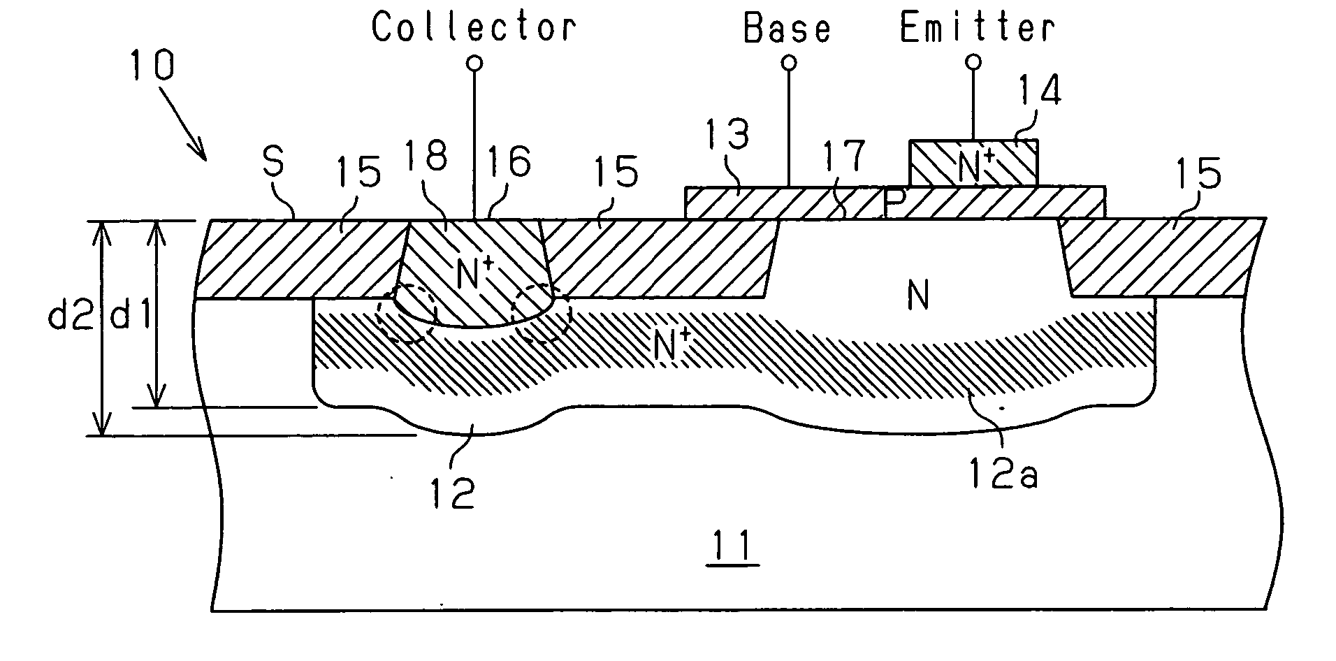
[0023] The structure of a bipolar transistor 10 included in a semiconductor device according to a preferred embodiment of the present invention will now be described.

[0024] Referring to FIG. 1, the bipolar transistor 10 is an NPN junction transistor. The bipolar transistor 10 includes an N-type conductive layer collector region 12, which is formed in the P-type silicon substrate 11 through ion implantation, and a P-type conductive layer base region 13 and an N-type conductive layer emitter region 14, which are formed on the collector region 12. The bipolar transistor 10 of the preferred embodiment is a vertical bipolar transistor in which the emitter region 14 is superimposed on the base region 13.

[0025] The collector region 12 includes a high concentration layer 12a, which is formed at a location spaced from a main surface S and has an especially high N-type impurity concentration. The high concentration layer 12a functions as a main conductive path in the collector region 12 dur...


PUM


Abstract

A semiconductor device including a bipolar transistor in which the collector resistance. The bipolar transistor includes a first conduction type semiconductor substrate having a main surface. A second conduction type collector region is formed in the semiconductor substrate. A shallow trench isolation structure isolates the main surface of the semiconductor substrate into two insulated active regions. A collector leading portion is formed in one of the active regions. A first conduction type base region and a second conduction type emitter region are formed on the other one of the active regions. The collector region has a first depth from the main surface immediately below the shallow trench isolation structure, and the collector region has a second depth from the main surface immediately below the two active regions. The first depth is less than the second depth.

Description

CROSS-REFERENCE TO RELATED APPLICATIONS [0001] This application is based upon and claims the benefit of priority from prior Japanese Patent Application No. 2005-100949, filed on Mar. 31, 2005, the entire contents of which are incorporated herein by reference. BACKGROUND OF THE INVENTION [0002] The present invention relates to a semiconductor device including a bipolar transistor and a method for manufacturing the same. [0003]FIG. 8 is a cross-sectional view showing the structure of a typical bipolar transistor described in, for example, Japanese Laid-Open Patent Publication No. 2004-87599. As shown in FIG. 8, the bipolar transistor 50 includes an N-type conductive layer collector region 52, which is formed in a P-type silicon substrate 51 through ion implantation, and a P-type conductive layer base region 53 and an N-type conductive layer emitter region 54, which are formed on a main surface S of the P-type silicon substrate 51. [0004] A shallow trench isolation (STI) structure 55 i...

Claims


Application Information

Patent Timeline
Patent Type & Authority Applications(United States)
IPC IPC(8): H01L29/788
CPCH01L29/0821H01L29/7322H01L29/66272
Inventor FUJIWARA, SHUJI
Owner SEMICON COMPONENTS IND LLC
Why Eureka
Try Eureka