Circuit and method for automatic gain control

a gain control and circuit technology, applied in the field of wireless communication systems, can solve the problems of not being able to achieve the certification of wireless cores for sale or use in standard-compliant wireless devices, the cost of manufacturing these rf devices can be prohibitive, and the manufacturing technology is relatively new

Active Publication Date: 2006-10-05
ICERA CANADA ULC
View PDF15 Cites 12 Cited by
  • Summary
  • Abstract
  • Description
  • Claims
  • Application Information

AI Technical Summary

Problems solved by technology

Such standards include EDGE and WCDMA communications standards for example, and failure to adhere to this particular aspect of such standards can result in non-certification of the wireless core for sale or use in standard-compliant wireless devices.
However, such manufacturing technologies are relatively new, very complex, and hence expensive.
Consequently, the costs for manufacturing these RF devices can be prohibitive.
Unfortunately, CMOS gain circuits do not exhibit a substantially linear characteristic between gain and the input control voltage VCONT.
Unfortunately, this technique for automatic adjustment of the gain is not suitable due to loading of the TX_OUT node by the feed back loop line to AGC 42.
This loading can cause distortion and loss of output signal strength, and is hence, undesirable.
This loading may also introduce noise in the TX signal which is also undesirable.
However, this technique is not effective for adjusting VGAIN properly in response to supply voltage, process and temperature variations.
More specifically, the range of adjustment is limited by virtue of the fact that the replica circuit may not be capable of detecting supply voltage, temperature and process variations due to the analog nature of the dummy circuit, which lacks reproducibility and controllability.

Method used


Image

  • Circuit and method for automatic gain control
  • Circuit and method for automatic gain control
  • Circuit and method for automatic gain control

Examples


Embodiment Construction

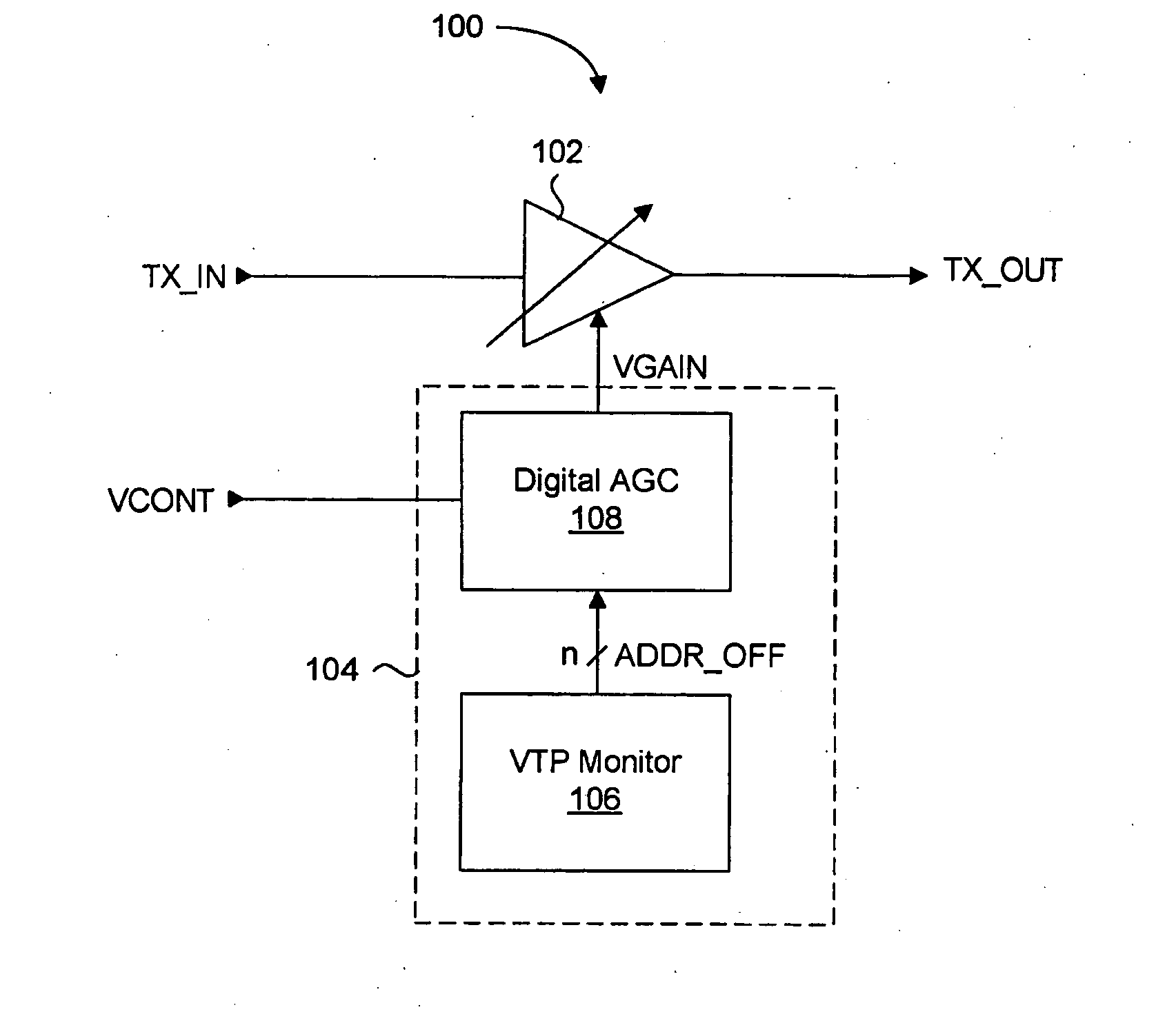
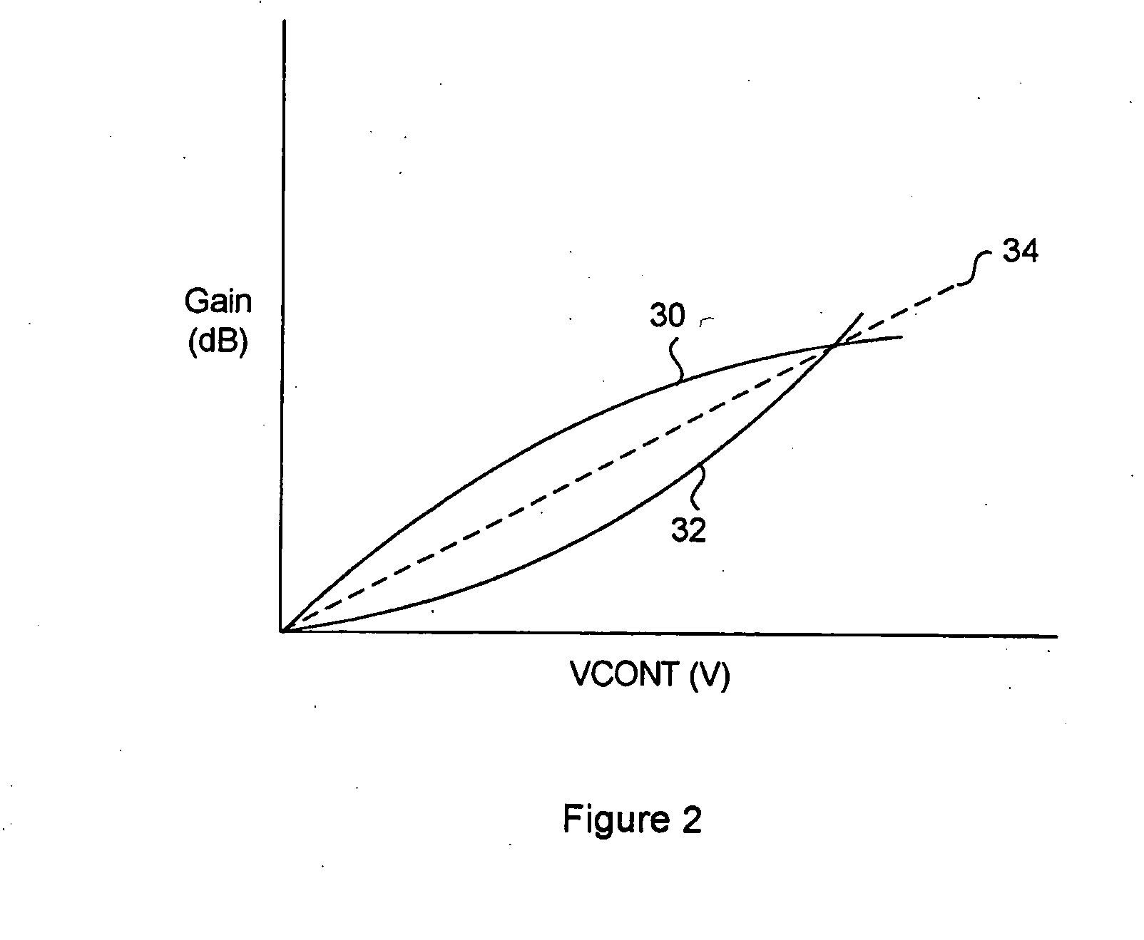
[0037] Generally, the present invention provides a system for generating a supply voltage, temperature and process compensated gain control voltage from a digital data word. In particular, the compensated gain voltage control maintains a substantially linear relationship between gain and an input control voltage for a gain circuit of a transmitter circuit. A monitor circuit senses at least one of the supply voltage, temperature and process parameters, and generates a first set of digital signals corresponding to the sensed parameter. A digital compensator circuit converts the input control voltage into a second set of digital signals, and decodes the combined first and second set of digital signals to access a memory for providing a data word. The data word is converted into an analog voltage representing the compensated gain voltage control signal. The parameters can be periodically sensed to update the first set of address signals in the event that any of the parameters have chang...


PUM


Abstract

A system for generating a supply voltage, temperature and process compensated gain control voltage from a digital data word. In particular, the compensated gain voltage control voltage maintains a linear relationship between a change in gain in response to an input gain control voltage for a gain circuit of a transmitter circuit. A monitor circuit senses at least one of the supply voltage, temperature and process parameters, and generates a first set of digital signals corresponding to the sensed parameter. A digital compensator circuit converts the input gain control voltage into a second set of digital signals, and decodes the combined first and second set of digital signals to provide a data word. The data word is converted into an analog voltage representing the compensated gain voltage control voltage. The digital compensator circuit includes a table of compensation values, each accessible by a distinct combination of the first and second set of digital signals.

Description

FIELD OF THE INVENTION [0001] The present invention relates generally to wireless communication systems. More particularly, the present invention relates to automatic gain control in wireless communication systems. BACKGROUND OF THE INVENTION [0002] Wireless devices have been in use for many years for enabling mobile communication of voice and data. Such devices can include mobile phones and wireless enabled personal digital assistants (PDA's) for example. FIG. 1 is a generic block diagram of the core components of such wireless devices. The wireless core 10 includes a baseband processor 12 for controlling application specific functions of the wireless device and for providing and receiving voice or data signals to a radio frequency (RF) transceiver chip 14. The RF transceiver chip 14 is responsible for frequency up-conversion of transmission signals, and frequency down-conversion of received signals. RF transceiver chip 14 includes a receiver core 16 connected to an antenna 18 for ...

Claims


Application Information

Patent Timeline
Patent Type & Authority Applications(United States)
IPC IPC(8): H03G3/10H04W52/52
CPCH03G3/3042H04W52/52H04B2001/0416
Inventor MANKU, TAJINDER
Owner ICERA CANADA ULC
Why Eureka
Try Eureka