
Flash memories and processing systems including the same

a technology of flash memory and processing system, which is applied in the direction of digital storage, data conversion, instruments, etc., can solve the problems of data loss, volatile memory, and the difficulty of users updating stored contents, so as to improve the read and/or write speed

Inactive Publication Date: 2006-10-05
SAMSUNG ELECTRONICS CO LTD
View PDF19 Cites 77 Cited by
  • Summary
  • Abstract
  • Description
  • Claims
  • Application Information

AI Technical Summary

Benefits of technology

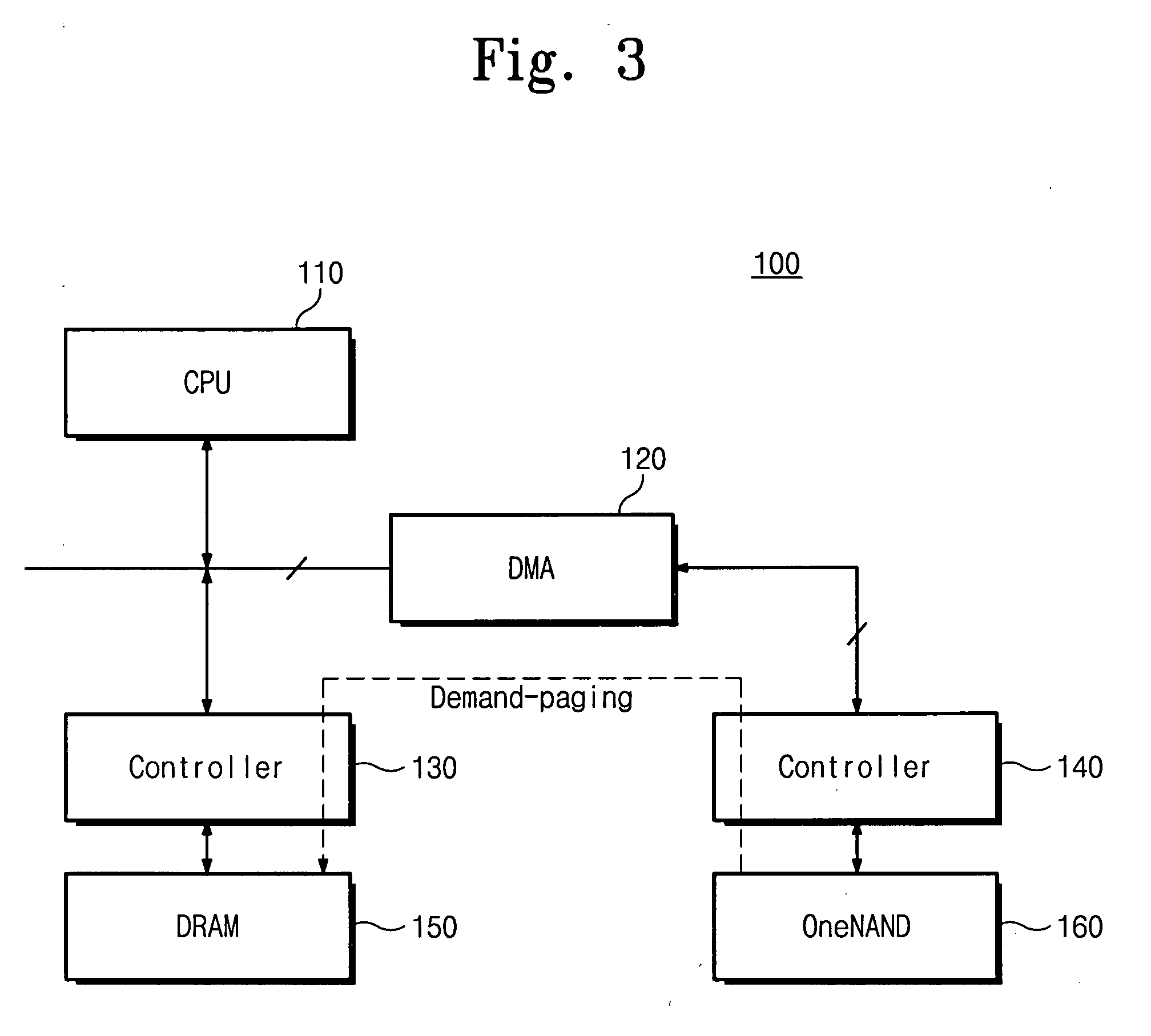
[0012] Example embodiments of the present invention provide a memory (e.g., a ONE13 NAND-type flash memory), which may improve read and / or write speed.

Problems solved by technology

Data may be lost when the power is turned off and hence, they are volatile memories.
Non-volatile memories, such as, MROM, PROM and / or EPROM may not be available (e.g., free) during erase and / or write operations, and it may be more difficult for users to update stored contents.
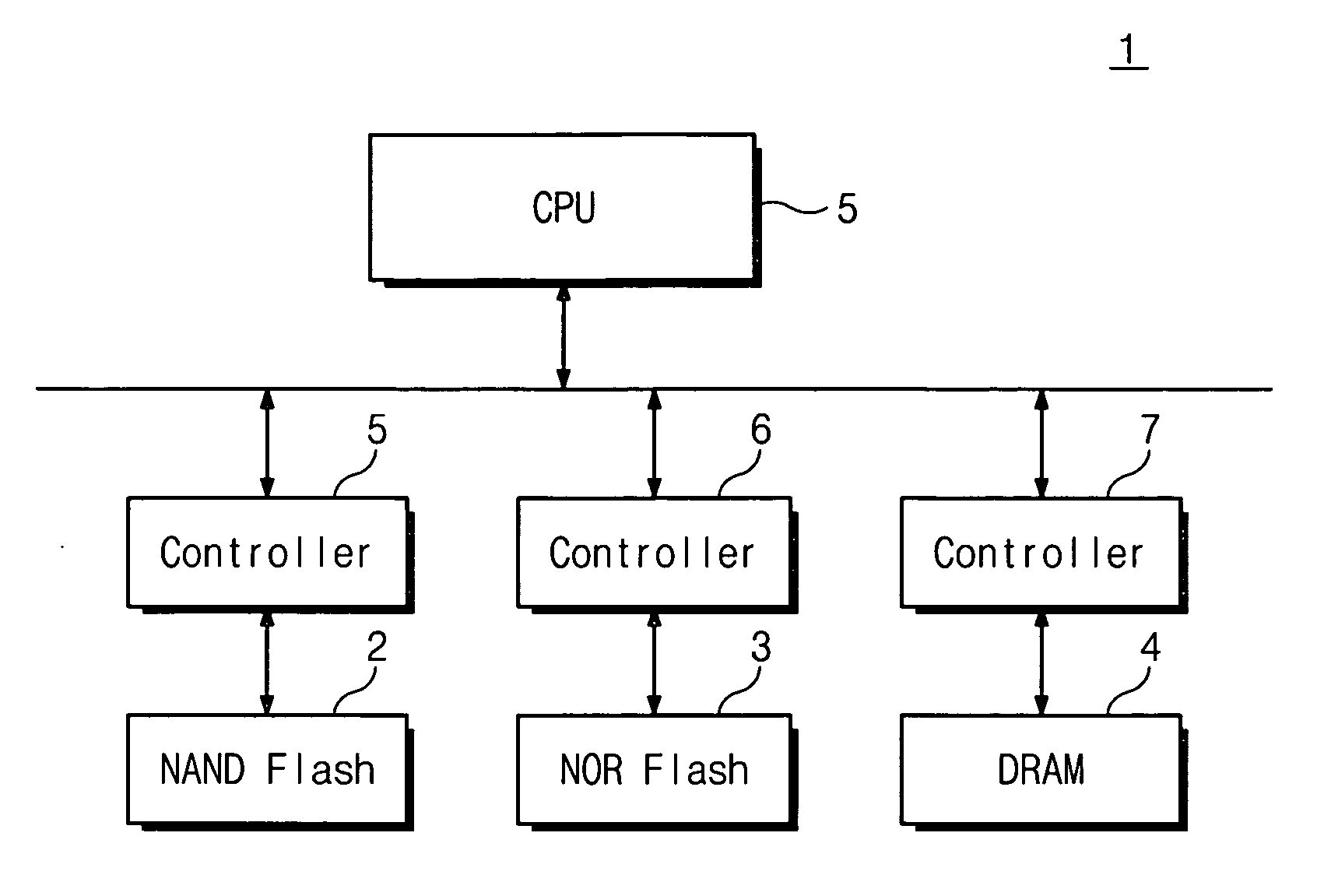
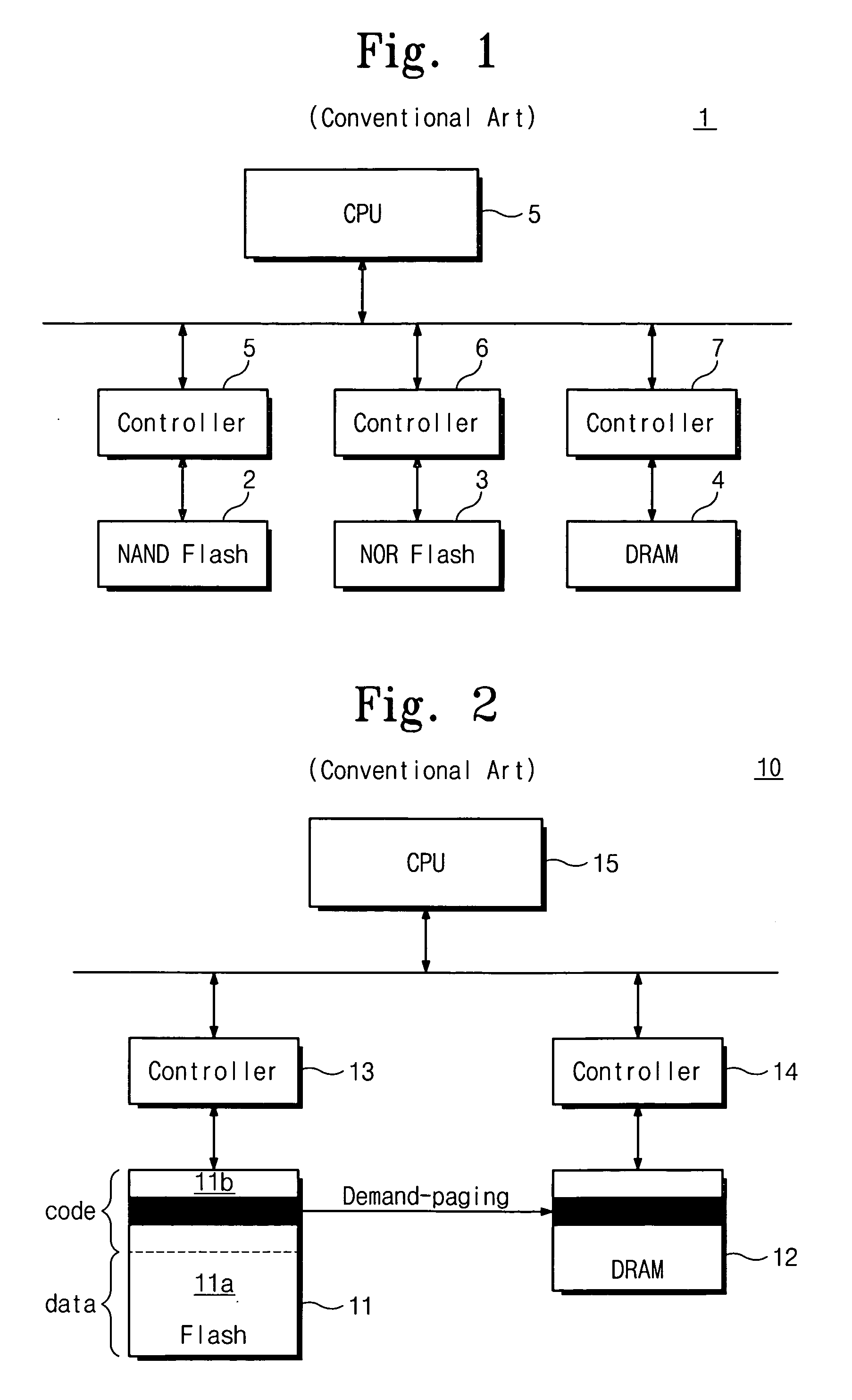
This architecture illustrated in FIG. 1 may result in an increase in manufacturing costs.
Moreover, since memory controllers 5, 6 and 7 may be required to control the NAND-type flash memory 2, the NOR-type flash memory 3 and the DRAM 4, respectively, the control of a system (e.g., bus architecture) may be more complex.

Method used


Image

  • Flash memories and processing systems including the same
  • Flash memories and processing systems including the same
  • Flash memories and processing systems including the same

Examples


Embodiment Construction

[0043] Various example embodiments of the present invention will now be described more fully with reference to the accompanying drawings in which some example embodiments of the invention are shown. In the drawings, the thicknesses of layers and regions are exaggerated for clarity.

[0044] Detailed illustrative embodiments of the present invention are disclosed herein. However, specific structural and functional details disclosed herein are merely representative for purposes of describing example embodiments of the present invention. This invention may, however, may be embodied in many alternate forms and should not be construed as limited to only the embodiments set forth herein.

[0045] Accordingly, while example embodiments of the invention are capable of various modifications and alternative forms, embodiments thereof are shown by way of example in the drawings and will herein be described in detail. It should be understood, however, that there is no intent to limit example embodi...


PUM


Abstract

A memory may include first and second buffer memories and a memory core. The memory core may include memory blocks each having a plurality of pages and a page buffer for reading data from a selected memory block. A control logic may control the first and second buffer memories and the memory core. The control logic may have a register for storing address and command information of the memory core. The control logic may control the memory core so that data read periods for pages of the selected memory block are carried out according to the stored address and command information. The control logic may control the first and second buffer memories and the memory core so that data in the page buffer may be transferred to the first and / or second buffer memories during the data read periods. The control logic may deactivate an interrupt signal when data in the page buffer is transferred to the first and / or second buffer memory and may activate the interrupt signal when data in the first and / or second buffer memory is transferred to an external storage.

Description

PRIORITY STATEMENT [0001] This non-provisional U.S. application claims priority under 35 U.S.C. §119 to Korean Patent Application No. 2005-27658 filed on Apr. 1, 2005 in the Korean Intellectual Property Office (KIPO), the entire contents of which are incorporated herein by reference. FIELD OF THE INVENTION [0002] Example embodiments of the present invention relate to semiconductor memory devices, for example, non-volatile semiconductor memory devices. BACKGROUND [0003] Semiconductor memories may be used in digital logic system designs, such as, computers and / or microprocessor-based applications. Examples of microprocessor-based applications are satellites, consumer electronics, and / or many other electronic devices. Advances in the fabrication of semiconductor memories including, for example, process enhancements and / or technology developments have been made through scaling of memories for higher densities and / or faster speeds. These advances have helped establish performance standar...

Claims


Application Information

Patent Timeline
IPC IPC(8): G06F5/00
CPCG11C7/1039G11C16/26G11C7/22G11C16/0483G11C16/32
Inventor CHO, HYUN-DUKCHOI, YOUNG-JOONKIM, TAE-GYUN
Owner SAMSUNG ELECTRONICS CO LTD
Learn More