
Semiconductor device capable of controlling OCD and ODT circuits and control method used by the semiconductor device

a technology of ocd and odt circuits, which is applied in the direction of logic circuits, pulse techniques, and reliability increasing modifications, etc., can solve the problems of device b>200/b>, the inability to alter the fixed external resistance, and the difficulty in precisely controlling the impedance of the ocd circui

Active Publication Date: 2006-10-12
SAMSUNG ELECTRONICS CO LTD
View PDF6 Cites 38 Cited by
  • Summary
  • Abstract
  • Description
  • Claims
  • Application Information

AI Technical Summary

Benefits of technology

[0024] According to an exemplary embodiment of the present invention, there is provided a method comprising: generating a control code in response to a control signal;

Problems solved by technology

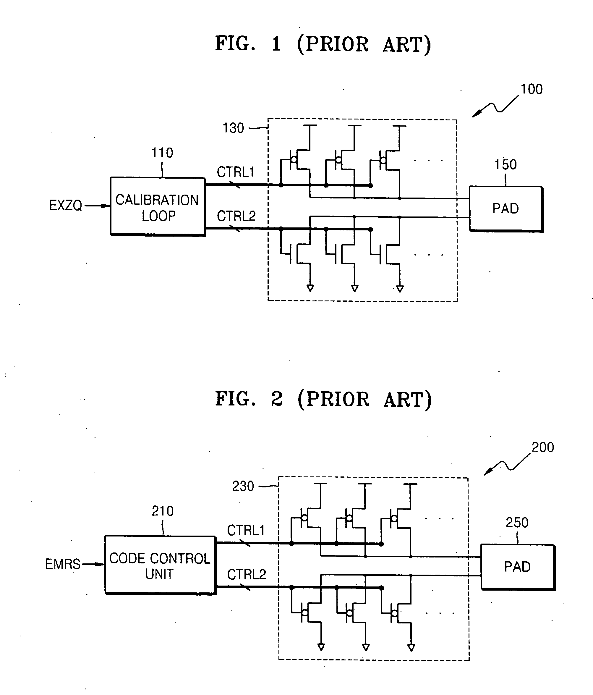
However, the semiconductor device 100 or 200 cannot alter the fixed external resistance even when the impedance of the OCD circuit needs to be adjusted to improve channel characteristics.
Thus, it is difficult to precisely control the impedance of the OCD circuit.
However, an increase in the number of bits of the external mode register set signal complicates the circuit structure of the semiconductor device 200.

Method used


Image

  • Semiconductor device capable of controlling OCD and ODT circuits and control method used by the semiconductor device
  • Semiconductor device capable of controlling OCD and ODT circuits and control method used by the semiconductor device
  • Semiconductor device capable of controlling OCD and ODT circuits and control method used by the semiconductor device

Examples


Embodiment Construction

[0031] Hereinafter, exemplary embodiments of the present invention will be described in detail with reference to the attached drawings. Like reference numerals in the drawings denote like elements, and thus their description will omitted.

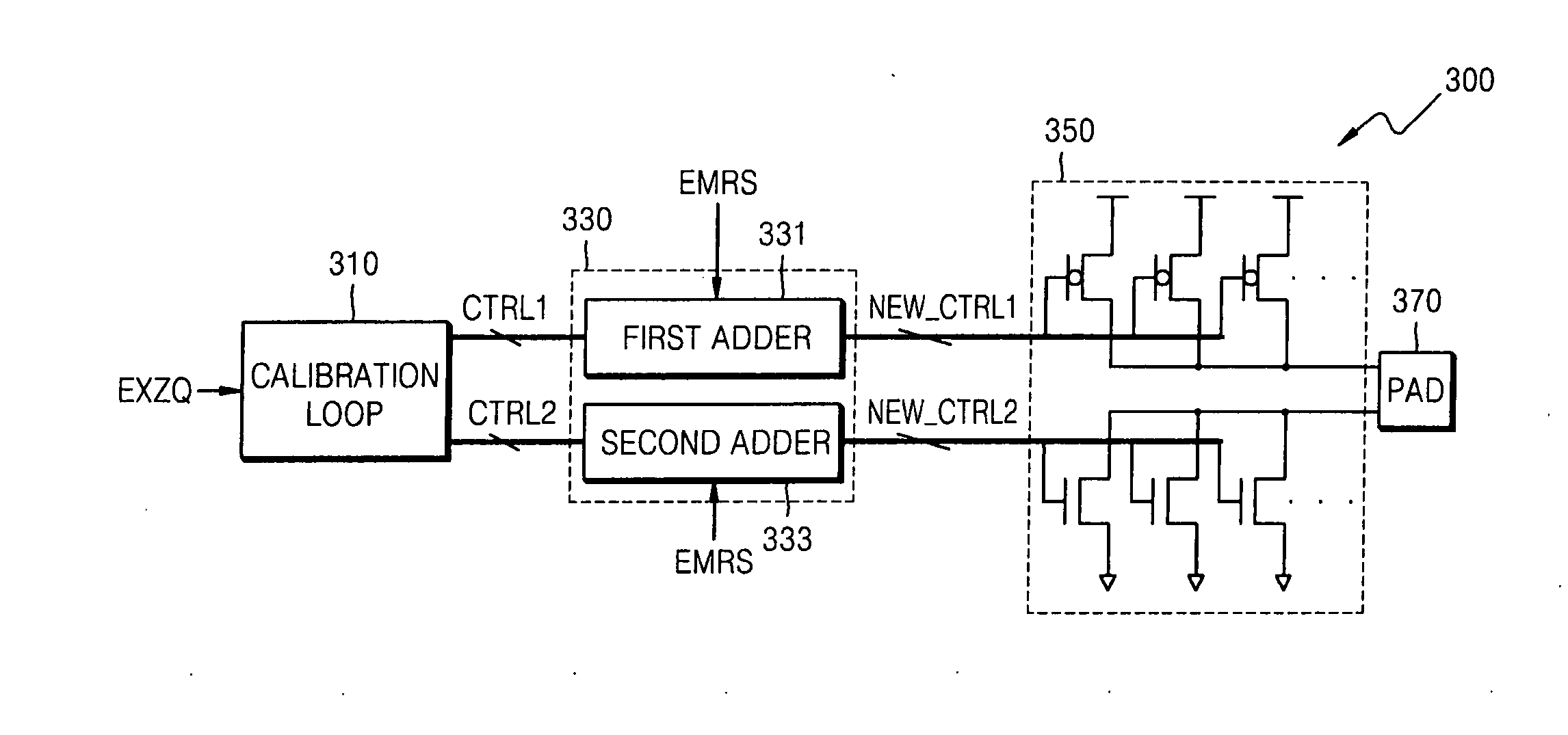
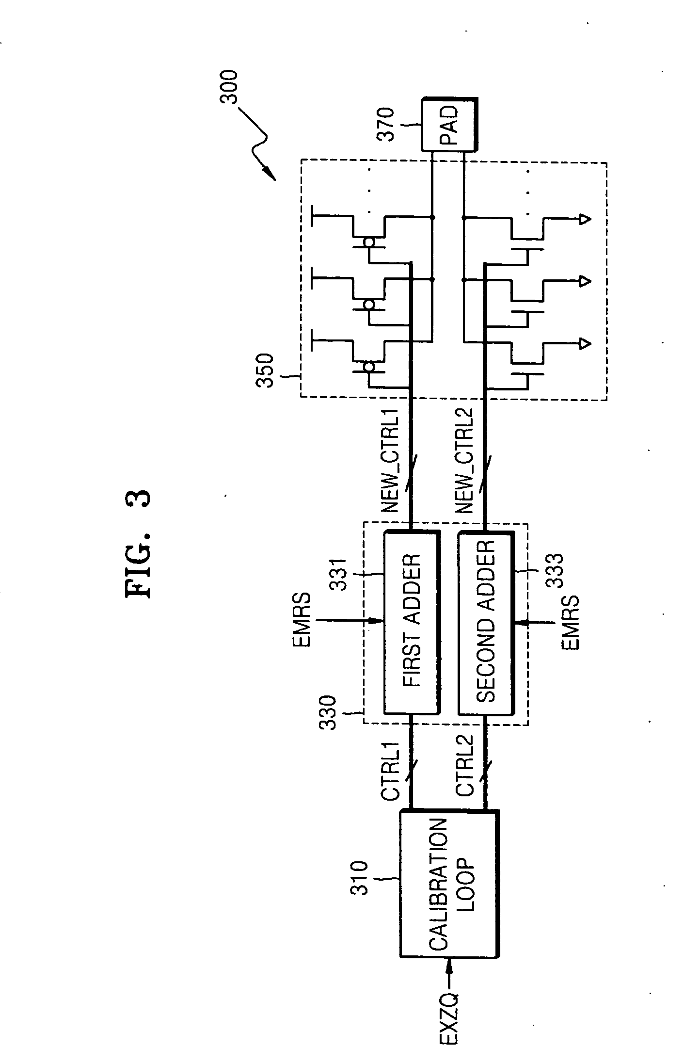
[0032]FIG. 3 is a block diagram of a semiconductor device 300 capable of controlling an off-chip-driver (OCD) circuit and an on-die-termination (ODT) circuit 350 according to an exemplary embodiment of the present invention. The semiconductor device 300 includes a calibration loop 310, an addition unit 330, the OCDT circuit 350, and a pad 370. The calibration loop 310 may be regarded as a control code generation unit generating first and second control codes CTRL1 and CTRL2 in response to a control signal EXZQ.

[0033] The control signal EXZQ is generated in response to reference resistance (not shown) external to the semiconductor device 300. The control signal EXZQ is input to the semiconductor device 300 through an input / output pin (not shown) in...


PUM


Abstract

Provided is a semiconductor device capable of controlling an on-die-termination (ODT) circuit and an off-chip-driver (OCD) circuit and a control method used by the semiconductor device. The semiconductor device includes a control code generation unit generating a control code in response to a control signal, an addition unit adding an adjustment code to the control code to produce an adjusted control code, and an ODT circuit, wherein an impedance of the ODT circuit is adjusted in response to the adjusted control code. The semiconductor device can adjust the control code more precisely by adding or subtracting the adjustment code to or from the control code. Accordingly, the impedance of an OCD circuit or ODT circuit can be adjusted more precisely.

Description

BACKGROUND OF THE INVENTION [0001] This application claims priority to Korean Patent Application No. 2005-0030432, filed on Apr. 12, 2005, in the Korean Intellectual Property Office, the disclosure of which is incorporated by reference herein. [0002] 1. Field of the Invention [0003] The present invention relates to a semiconductor device and a control method used by the same, and more particularly, to a semiconductor device capable of precisely controlling an on-die-termination (ODT) circuit and an off-chip-driver (OCD) circuit and a method of controlling the same. [0004] 2. Description of the Related Art [0005] The effects of the flow of data, data strobes, and AC parameters related to input and output of addresses and control signals have become increasingly more critical to the design of high-frequency double data rate (DDR) semiconductor devices. The electrical characteristics of a channel connecting two or more components, e.g., a DRAM or a CPU, can often be more important than...

Claims


Application Information

Patent Timeline
IPC IPC(8): H03K19/003
CPCH03K19/0005B26D3/24B26D3/30B26D1/60B26D2210/02
Inventor LEE, WOO-JINPARK, KWANG-ILKIM, HYUN-JINJANG, SEONG-JIN
Owner SAMSUNG ELECTRONICS CO LTD
Learn More