Multi-point correlated sampling for image sensors

Active Publication Date: 2006-10-19
APTINA IMAGING CORP
View PDF11 Cites 18 Cited by
  • Summary
  • Abstract
  • Description
  • Claims
  • Application Information

AI Technical Summary

Benefits of technology

[0014] The present invention provides in various method and apparatus exemplary embodiments an improved PPS circuit and method of operating it that integrates leakage onto an integrator amplifier during sampling periods. The method and apparatus of the present invention provides improved correlated sampling for the reduction of kTC and dark integration noise, such as bus leakage and blooming from pixel rows.
[0015] The above and other f

Problems solved by technology

This occurred in part because historically, PPS had gained a negative reputation as being inferior with respect to fixed pattern noise (“FPN”) and noise due to reduced readout sensitivity and column line leakage.
As a result, charge-coupled devices (“CCDs”) were favored over CMOS image sensors having PPS, notwithstanding that the manufacturing process for CCDs was much more costly than that for CMOS devices.
This is undesirable.
Low feedback capacitance, however, results in kTC noise.
This is undesirable.
Such leakage (e.g., “dark integration”) is primarily due to charge leakage in a row being read out, but may also arise fro

Method used


Image

  • Multi-point correlated sampling for image sensors
  • Multi-point correlated sampling for image sensors
  • Multi-point correlated sampling for image sensors

Examples


Embodiment Construction

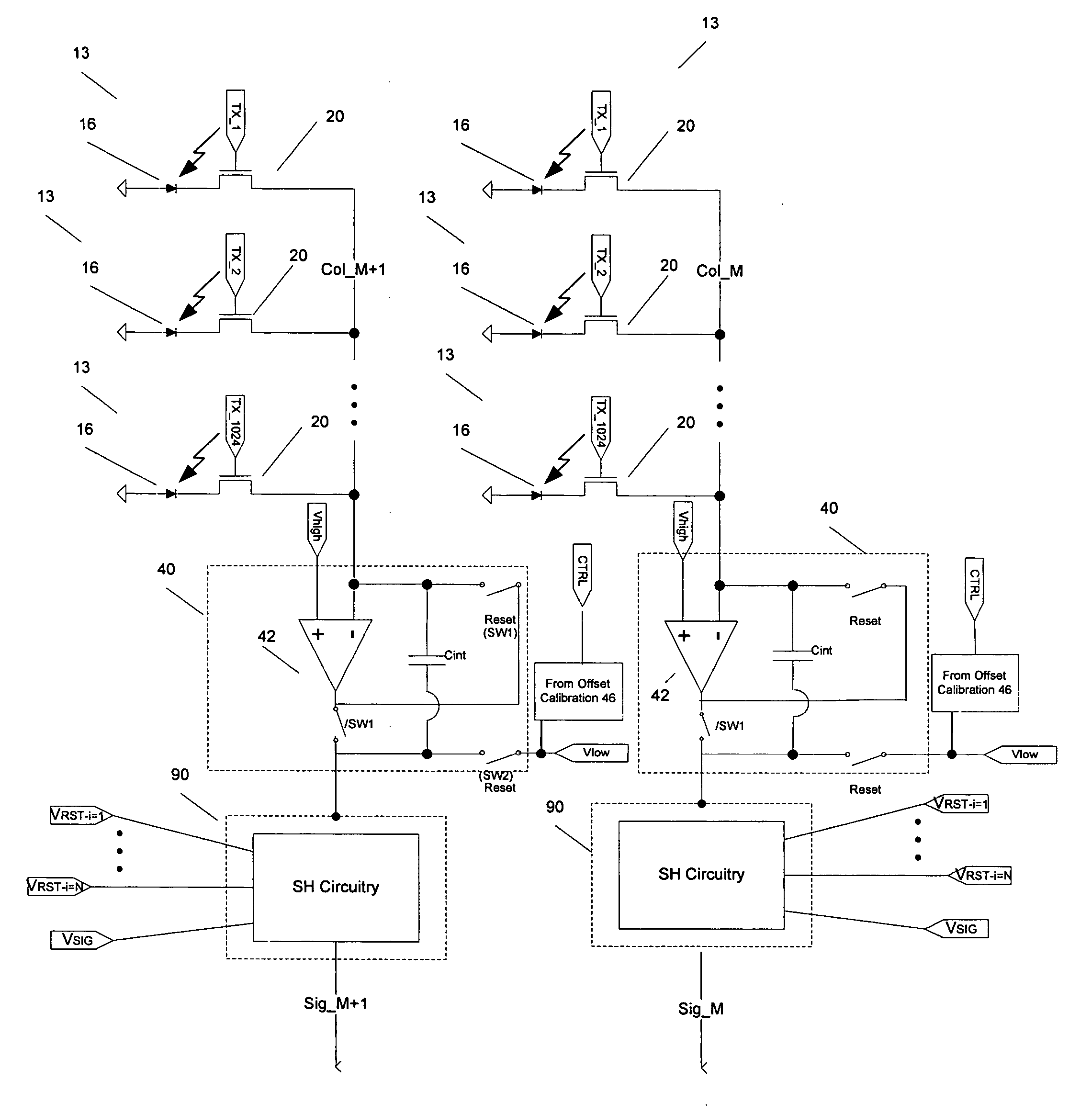
[0029] In the following detailed description, reference is made to the accompanying drawings which form a part hereof, and which illustrate specific embodiments of the present invention. These embodiments are described in sufficient detail to enable those of ordinary skill in the art to make and use the invention. It is also understood that structural, logical, or procedural changes may be made to the specific embodiments disclosed without departing from the spirit and scope of the present invention. The following detailed description is not to be taken in a limiting sense, and the scope of the present invention is defined only by the appended claims.

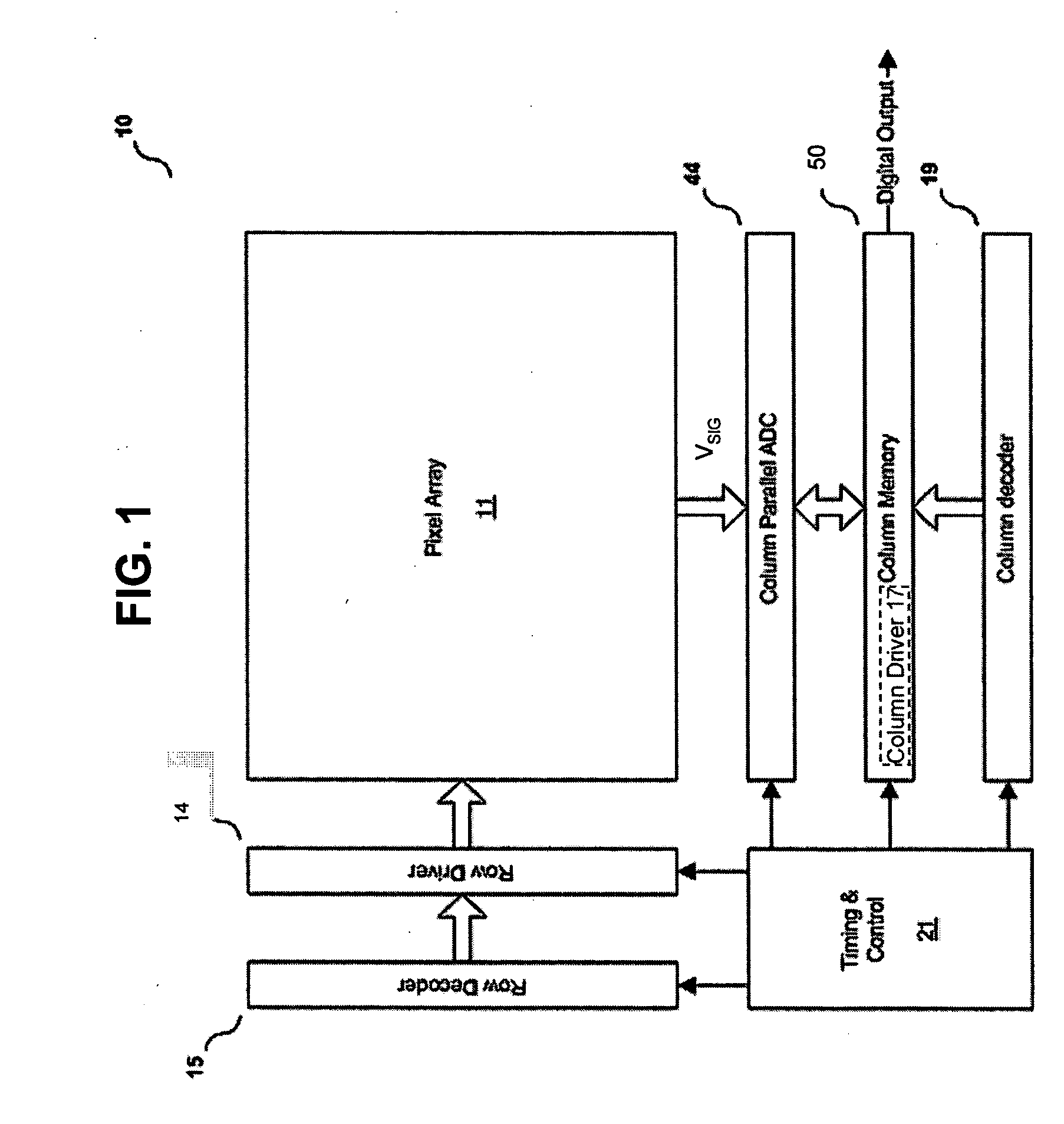
[0030]FIG. 1 illustrates a block diagram for a CMOS imager 10. The imager 10 includes a pixel array 11. The pixel array 11 comprises a plurality of pixels arranged in a predetermined number of columns and rows. The pixels of given rows in array 11 are all turned on at the same time by row select lines and the pixels of a given column a...


PUM


Abstract

An improved passive pixel sensor (PPS) circuit comprising a correlated sampling circuit and method that integrates pixel charge leakage onto an integrating amplifier during sampling periods. An integrator circuit is provided for integrating PPS pixel charges received via a column line, and correlated sampling circuit is provided for the removal of kTC noise and dark integration. A multi-point sampling of the output of the integrator is provided wherein at least a first and second correlated sample are used to detect the charge integration from the column line leakages, and at least a third sample is used to detect the PPS signal after pixel readout. The correlated sampling method is employed to remove kTC noise and dark integration from the PPS signal.

Description

FIELD OF THE INVENTION [0001] The present invention relates generally to passive pixel sensor image devices and to correlated sampling methods for the same. BACKGROUND OF THE INVENTION [0002] Image sensors typically employ light detecting elements (e.g., photosensors) and are used in various applications. Such image sensors may be formed using a variety of fabrication techniques. Currently, two commonly fabricated image sensors are CMOS image sensors and charge coupled device (CCD) image sensors. Each sensor generally includes an array of pixels containing the photosensors. The image sensors typically use photosensors in the form of photogates, phototransistors or photodiodes. [0003] When an image is focused on the image sensor array (also called an “imager array” or “pixel array”), light corresponding to the image is directed to the pixels usually through micro-lenses. Each micro-lens may be used to direct incoming light through a circuitry region of the corresponding pixel to the ...

Claims


Application Information

Patent Timeline
IPC IPC(8): H01L27/00H04N5/359H04N5/361H04N5/363H04N5/374H04N5/378
CPCH04N5/3592H04N5/3575H04N25/616H04N25/622H04N25/60H04N25/76H04N25/75
Inventor BOEMLER, CHRISTIAN
Owner APTINA IMAGING CORP
Why Eureka
Try Eureka