Image sensor module package

a technology of image sensor and module, applied in the direction of photoelectric discharge tubes, instruments, electric discharge lamps, etc., can solve the problem that the image sensor package b>100/b> cannot have a better electrical performance, and achieve the effect of enhancing the electrical performance of the image sensor chip, wide spacing, and small spacing

Inactive Publication Date: 2006-10-19
CHIPMOS TECH INC
View PDF7 Cites 35 Cited by
  • Summary
  • Abstract
  • Description
  • Claims
  • Application Information

AI Technical Summary

Benefits of technology

[0016] The bumped image sensor chip 320 is flip-chip attached to the second surface 312 of the glass substrate 310. The image sensor chip 320 has an active surface 321 which includes a sensing area 322. A plurality of bumps 323 are formed on the active surface 321 and are electrically connected the image sensor chip 320 to the via-redistribution layer 315. The sensing area 322 is aligned with the light entering area 313 on the first surface 311. An encapsulant 324 is used to seal the bumps 323. Preferably, the via-redistribution layer 315 is a fan-out design from the bumps323. The passive components 330 are disposed on the second surface 312 of the glass substrate 310 to enhance the electrical performance of the image sensor chip 320. In this embodiment, the FPC 340 is bonded to the connecting pads 314 to transmit the signals of the image sensor chip 320.
[0017] Since the via-redistribution layer 315 is fan-out from the bumps 323 of the image sensor chip 320, the vias 316 have enough pitches to be formed in the glass substrate 310 by laser drilling. Moreover, the via-redistribution layer 315 is electrically connected to the connecting pads 314 through the vias 316, therefore, the via-redistribution layer 315 will have more space to place passive components 330 on the second surface 312 of the glass substrate 310 and the image sensor module package 300 will not have the electrical interference due to the passive components 330. Furthermore, when connecting the FPC 340, the connecting pads 314 are formed on one side of the light entering area 313 so that connecting pads 314 can have wider spacing to electrically connect to the FPC 340 to avoid electrical interference due to smaller spacing of the connecting pads 314.

Problems solved by technology

Furthermore, the glass substrate 110 doesn't have enough space for placing passive components so that the image sensor package 100 cannot have a better electrical performance.

Method used


Image

  • Image sensor module package
  • Image sensor module package
  • Image sensor module package

Examples


first embodiment

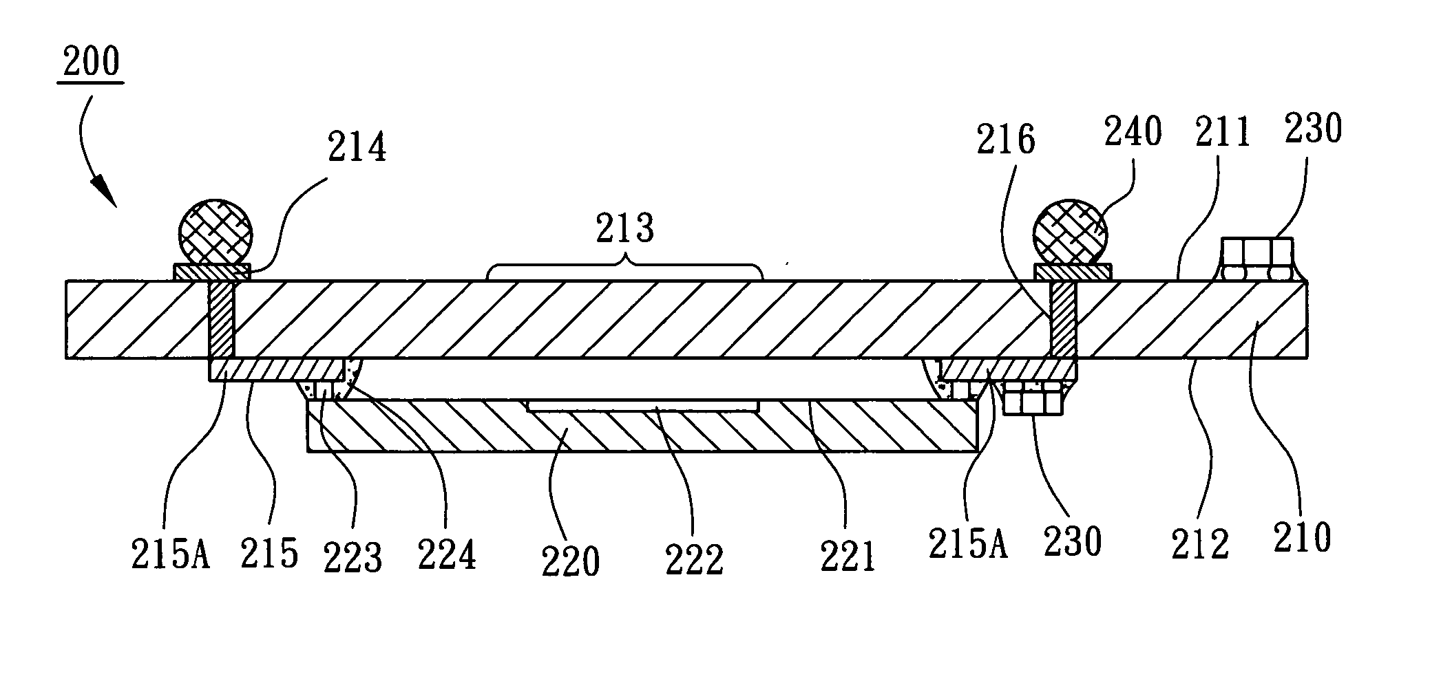
[0012] According to the present invention, as shown in FIG. 2, an image sensor module package 200 comprises a glass substrate 210, a bumped image sensor chip 220, and a plurality of passive components 230 where the glass substrate 210 has a first surface 211 and an opposing second surface 212. A light entering area 213 is defined in the first surface 211. Moreover, the glass substrate 210 includes a plurality of connecting pads 214, a via-redistribution layer 215, and a plurality of vias 216 where the connecting pads 214 are formed on the first surface 211 of the glass substrate 210 and located outside the light entering area 213. The via-redistribution layer 215 is formed on the second surface 212 without blocking the light entering area 213 where the via-redistribution layer 215 has a plurality of fan-out pads 215A connected with traces in a fan-out design to redistribute the locations of the vias 216 with a larger pitch. The vias 216 are formed in the glass substrate 210 penetrat...

second embodiment

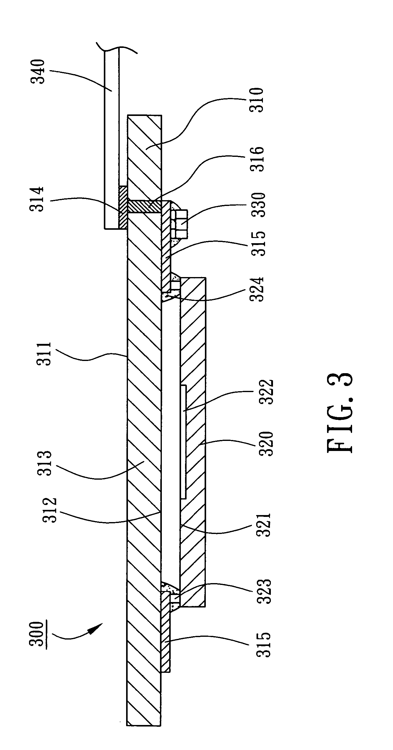
[0015] According to the present invention, as shown in FIG. 3, an image sensor module package 300 comprises a glass substrate 310, a bumped image sensor chip 320, a plurality of passive components 330, and a flexible printed circuit 340 (FPC) where the glass substrate 310 has a first surface 311 and an opposing second surface 312. A light entering area 313 is defined on the first surface 311. The glass substrate 310 includes a plurality of connecting pads 314, a via-redistribution layer 315, and a plurality of vias 316 where the connecting pads 314 are formed on the first surface 311 and located outside the light entering area 313 of the glass substrate 310. The connecting pads 314 are formed on the second surface-312 and electrically connected to the via-redistribution layer 315 through the vias 316.

[0016] The bumped image sensor chip 320 is flip-chip attached to the second surface 312 of the glass substrate 310. The image sensor chip 320 has an active surface 321 which includes a ...


PUM


Abstract

An image sensor module package is disclosed. A plurality of connecting pads are formed on a first surface of a glass substrate having and located outside a light entering area. A via-redistribution layer is formed on an opposing second surface of the glass substrate. A plurality of vias penetrate the glass substrate to electrically connect the via-redistribution layer with the connecting pads. A bumped image sensor chip is flip-chip attached to the second surface of the glass substrate so that a sensing area of the image sensor chip is corresponding to a light entering area of the glass substrate without blocking the via-redistribution layer. The connecting pads may connect to a plurality of solder balls or a FPC. In one embodiment, a plurality of passive components can be placed on the via-redistribution layer to enhance the electrical performance and the functions of the image sensor module package.

Description

FIELD OF THE INVENTION [0001] The present invention relates to an image sensor module package, and more particularly, to an image sensor module package by flip-chip attaching an image sensor chip to a glass substrate. BACKGROUND OF THE INVENTION [0002] Image sensor devices have been widely implemented in everyday lives such as cellular phones, personal digital assistants (PDA), digital still cameras (DSC), digital video cameras (DV), video phones, video conferences, and so on. In order to meet the needs of the consumers, there are more requirements for image qualities and functions. [0003] One kind of image sensor package is COG (Chip-On-Glass) type. As shown in FIG. 1, a conventional image sensor package 100 comprises a glass substrate 110, a bumped image sensor chip 120, an encapsulant 130 and a plurality of solder balls 140. The glass substrate 110 has a first surface 111 and a second surface 112 where the first surface 111 has a light entering area 113. Moreover, the glass subst...

Claims


Application Information

Patent Timeline
Patent Type & Authority Applications(United States)
IPC IPC(8): H01J5/02
CPCH01L27/14618H01L2224/16H01L2924/00011H01L2924/00014H01L2924/15311H01L2224/0401
Inventor CHAO, YEONG-CHINGLIU, AN-HONGHUANG, HSIANG-MINGLEE, YI-CHANGLEE, YAO-JUNG
Owner CHIPMOS TECH INC
Why Eureka
Try Eureka