Liquid crystal display and drive circuit thereof

a technology of drive circuit and liquid crystal display, which is applied in the direction of instruments, static indicating devices, etc., can solve the problems of circuit area expansion, large panel size, and required area, and achieve the effect of reducing the size of the data line drive circui

Active Publication Date: 2006-10-19
RENESAS ELECTRONICS CORP
View PDF6 Cites 60 Cited by
  • Summary
  • Abstract
  • Description
  • Claims
  • Application Information

AI Technical Summary

Benefits of technology

[0012] The present invention reduces a size of ...

Problems solved by technology

However we have now discovered that there are some problems in the conventional circuit described as above.
A first problem is that an area is required for placing data line drive circuits on an upper and a ...

Method used


Image

  • Liquid crystal display and drive circuit thereof
  • Liquid crystal display and drive circuit thereof
  • Liquid crystal display and drive circuit thereof

Examples


first embodiment

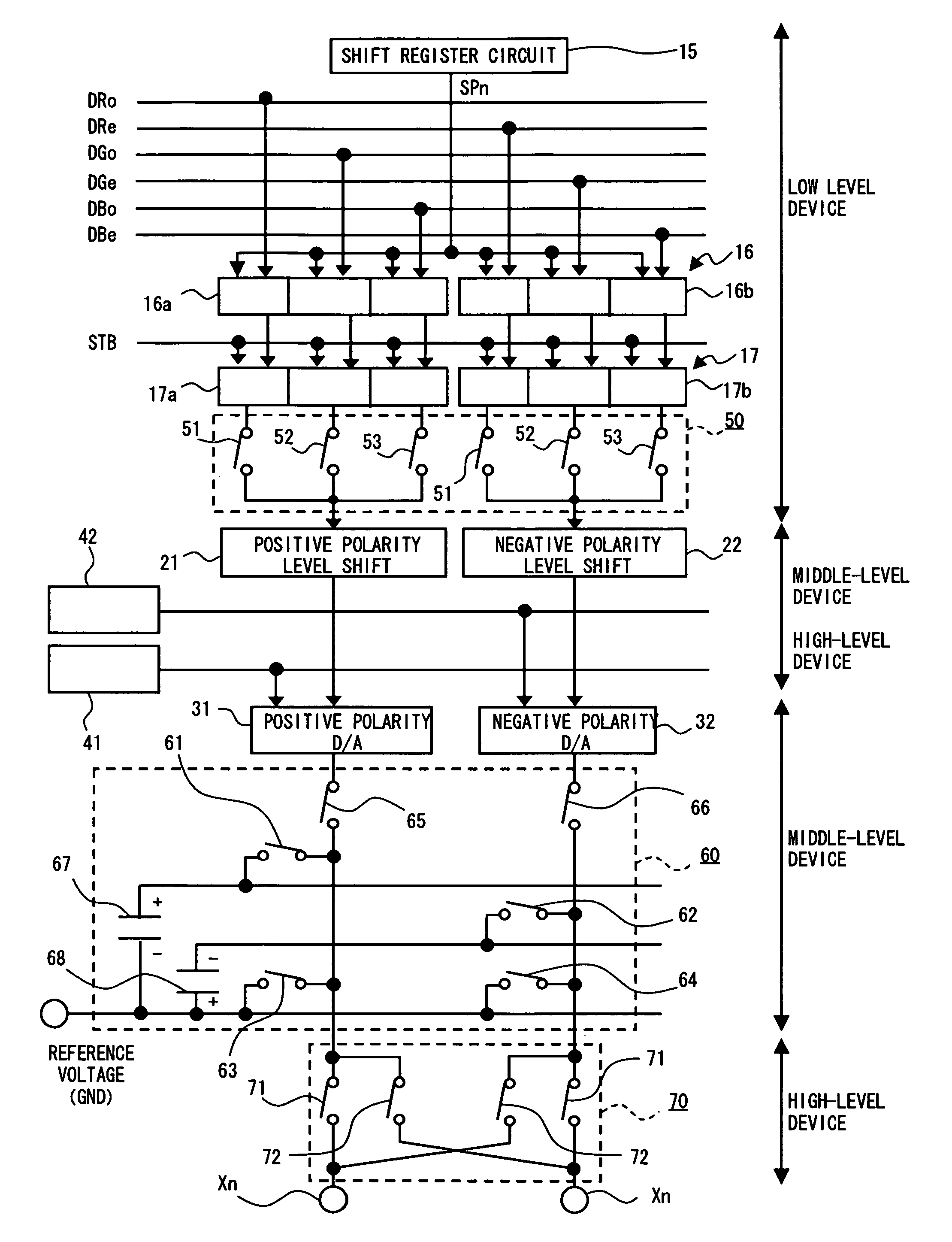
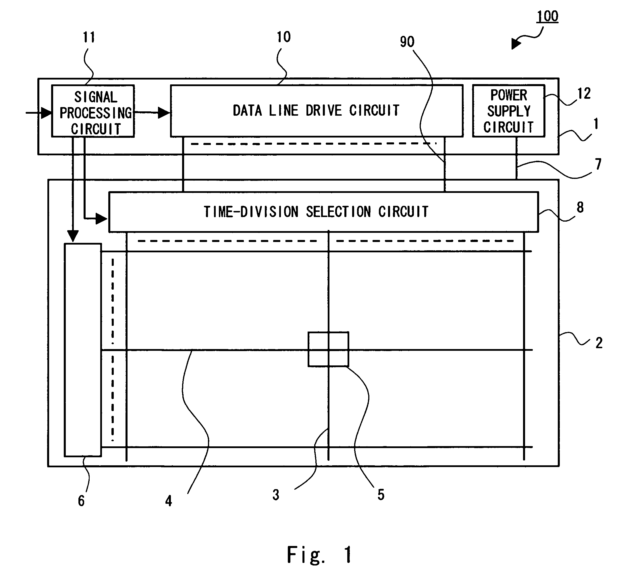
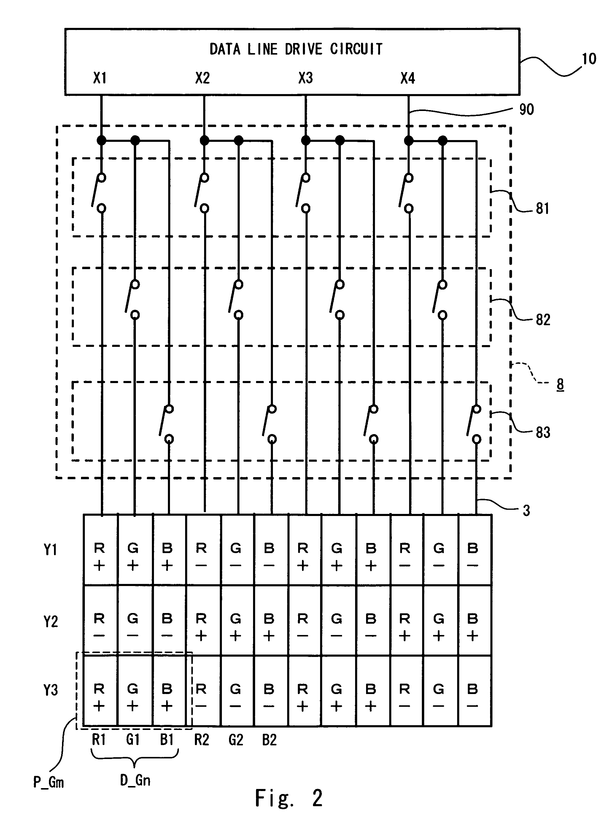
[0032]FIG. 1 is a block diagram showing a liquid crystal display 100 of this embodiment. The liquid crystal display 100 of this embodiment includes a plurality of scan lines 4, a plurality of data lines 3, and pixels 5 provided at each intersection of the plurality of scan lines 4 and the plurality of data lines 3. The liquid crystal display 100 further includes a plurality of pixel groups comprised of pixels 5 which is provided at each intersection of the consecutive plurality of data line 3 and one of the plurality of scan lines 4. Signals of the same polarity are outputted to all data lines included in each of the plurality of pixel groups by a time-sharing drive that sequentially outputs signals, and reversed polarity signals are outputted to the plurality of pixel groups adjacent to each other, and signals with inversed polarity are outputted to the data lines included in the pixel groups.

[0033] That is, as illustrated in FIG. 1, a plurality of data lines 3 and a plurality of ...

second embodiment

[0082] In the first embodiment, the polarity switching circuit 70 is formed on the driver IC1 and the time-sharing selection circuit 8 is formed on a panel. However a selection circuit having polarity switching function along with time-sharing switch function may be formed on the panel. FIG. 12 is a detailed diagram of a D / A conversion circuit portion and a precharge circuit portion of a driver IC1 according to this embodiment.

[0083] In the first embodiment, the polarity switching circuit 70 is provided between the precharge circuit 60 and output terminals Xn. However in this embodiment, the precharge circuit 60 is directly connected with output terminals Xn. As illustrated in FIG. 13, a time-sharing selection circuit 8 is comprised of two switches for each data line 3. Each switch is connected to an odd-numbered output terminal and an even-numbered output terminal, including a polarity switching function. Consequently, the number of switches constituting the time-sharing selection...

third embodiment

[0095] In the second embodiment, a selection circuit having a polarity switching function and a time-sharing switching function is formed on a panel. A charge recycling circuit may further be formed on the panel.

[0096]FIG. 15 is a block diagram showing a liquid crystal display 200 of this invention. A charge recycling circuit 9 is further formed on a liquid crystal panel substrate 2. A charge recycling circuit 9 is controlled by a signal outputted a the signal processing circuit 11 on a driver IC1. The charge recycling circuit 9 is described hereinafter in detail in reference to FIG. 16. In the charge recycling circuit 9, two charge recycling switches 91 and 92 are provided in parallel to each data lines 3, and other end of the charge recycling switches 91 and 92 are connected to a collection line 95 or a collection line 96 by each data line group. The collection lines 95 and 96 are respectively connected to a charge recycling capacities 93 and 94. The charge recycling switches 91 ...


PUM


Abstract

A liquid crystal display of this invention includes a plurality of scan lines, a plurality of data lines, and pixels provided at each intersection of the plurality of scan lines and the plurality of data lines. The liquid crystal display further includes a plurality of pixel groups constituted of the pixels provided at each intersection of the consecutive plurality of data lines and one of the plurality of scan lines, in which signals of the same polarity are outputted to all data lines included in each of the plurality of pixel groups by a time-sharing drive that sequentially outputs signals, and reversed polarity signals are outputted to the plurality of pixel groups adjacent to each other, so that signals with polarities inverted after each frame are outputted to the data lines included in the pixel groups.

Description

BACKGROUND OF THE INVENTION [0001] 1. Field of the Invention [0002] The present invention relates to a liquid crystal display and a drive circuit thereof that is suitable for placing a data line drive circuit having D / A conversion circuits only on one side of a panel for dot inversion drive. [0003] 2. Description of Related Art [0004] In a well-known liquid crystal display, a polarity of a voltage applied from a data line to a pixel via a TFT (hereinafter referred to as a pixel voltage) is inverted after each prescribed period. That means that pixels are AC driven. The polarity here indicates a positive or negative polarity of a pixel voltage with respect to a voltage of a common electrode of the liquid crystals (com voltage) as a reference. Such a drive method uses for inhibiting the degradation of liquid-crystal material. [0005] For the drive method, there are known methods such as dot inversion drive method and 2H dot inversion method. In the dot inversion drive method, polaritie...

Claims


Application Information

Patent Timeline
IPC IPC(8): G09G3/36
CPCG09G3/3614G09G3/3688G09G2310/0235G09G2320/0219G09G2310/027G09G2310/0297G09G2310/0248
Inventor HASHIMOTO, YOSHIHARU
Owner RENESAS ELECTRONICS CORP
Why Eureka
Try Eureka