Method of forming capacitor of semiconductor device by successively forming a dielectric layer and a plate electrode in a single processing chamber

Inactive Publication Date: 2006-10-19
SK HYNIX INC
View PDF9 Cites 3 Cited by
  • Summary
  • Abstract
  • Description
  • Claims
  • Application Information

AI Technical Summary

Benefits of technology

[0007] Accordingly, the present invention has been made to solve the above-mentioned problems occurring in the prior art, and an obje

Problems solved by technology

However, the above conventional method involves complicated processes, which generally take a long period of time because each of the storage electrode material, dielectric layer, and plate electrode material must be deposited in different chambers.
Whenever a substrate is transferred from on

Method used


Image

  • Method of forming capacitor of semiconductor device by successively forming a dielectric layer and a plate electrode in a single processing chamber
  • Method of forming capacitor of semiconductor device by successively forming a dielectric layer and a plate electrode in a single processing chamber

Examples


Embodiment Construction

[0028] Hereinafter, preferred embodiments of the present invention will be described with reference to the accompanying drawings. In the following description and drawings, the same reference numerals are used to designate the same or similar components, and so repetition of the description on the same or similar components will be omitted.

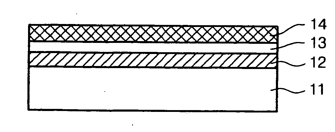
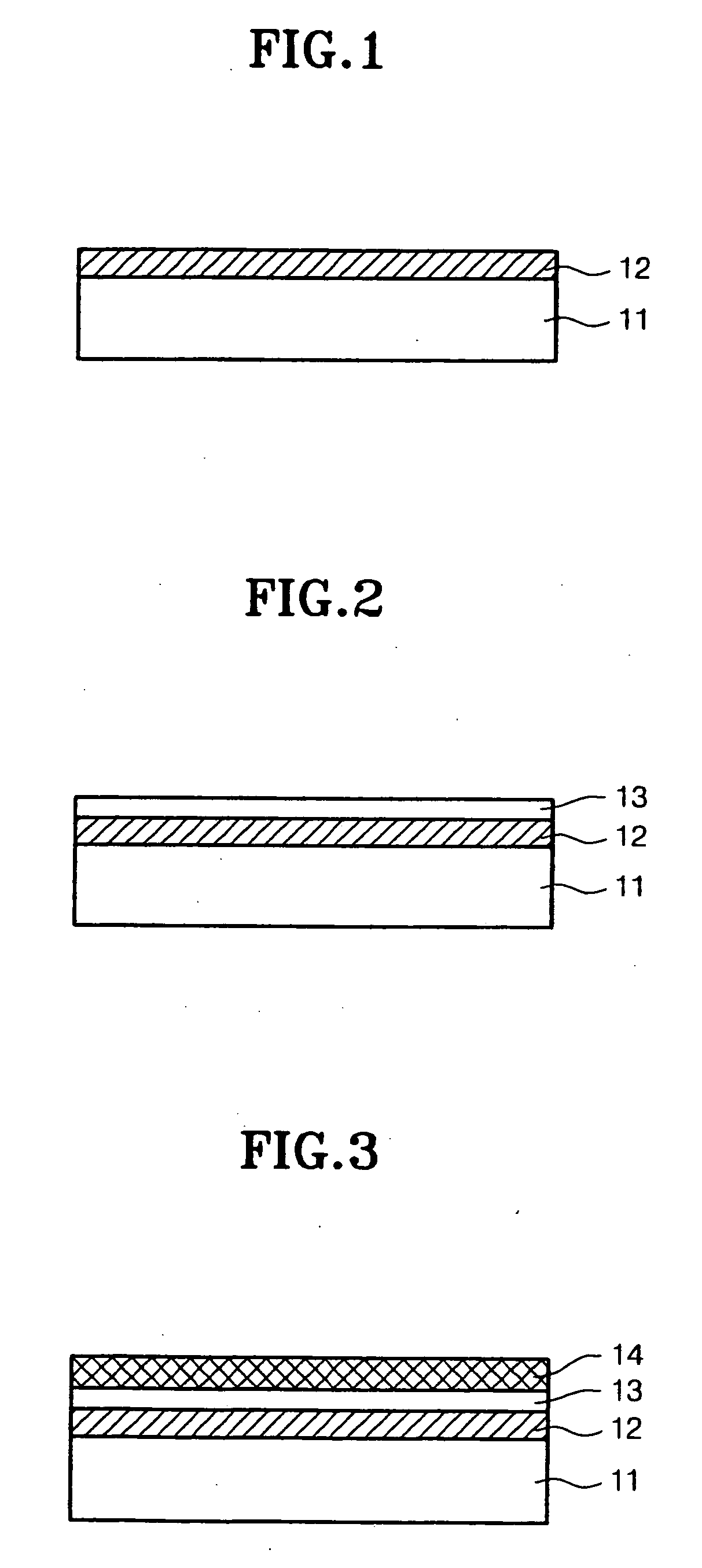
[0029] FIGS. 1 to 3 are cross-sectional views showing the processes in a method of forming a capacitor in a semiconductor device according to an embodiment of the present invention.

[0030] Referring to FIG. 1, a storage electrode 12 is formed on a semiconductor substrate 11, which has a primer layer formed thereon, using n+ doped polysilicon or any metal selected from TiN, Ru, Pt, Ir, HfN, and ZrN with a thickness of 50-500 Å. After the storage electrode 12 is formed, the substrate is cleaned to remove native oxide layers from surfaces of the storage electrode 12.

[0031] In the cleaning process, HF or BOE solution is used if the storage electrode...


PUM


Abstract

A capacitor in a semiconductor device is formed by successively forming a dielectric layer and a plate electrode in a single chamber according to an ALD process. The method includes the steps of forming a storage electrode on a semiconductor substrate; loading the semiconductor substrate into an ALD chamber with the storage electrode formed thereon; forming a metal oxide dielectric layer on the storage electrode in the chamber according to an ALD process; and successively forming a metal plate electrode on the metal oxide dielectric layer in the same chamber according to the ALD process.

Description

BACKGROUND OF THE INVENTION [0001] 1. Field of the Invention [0002] The present invention relates generally to a method for manufacturing a capacitor of a semiconductor device, and more particularly to a method for forming a capacitor of a semiconductor device capable of successively forming a dielectric layer and a plate electrode in a single ALD (atomic layer deposition) process chamber. [0003] 2. Description of the Prior Art [0004] A capacitor acts as a memory site for storing predetermined data in a memory device, such as a DRAM, and has a dielectric layer interposed between a storage electrode and a plate electrode. [0005] According to prior art, a conventional capacitor is formed by depositing a storage electrode material on a substrate in a chamber, and then the substrate is transferred to another chamber to deposit a dielectric layer on the storage electrode material, and then again the substrate is transferred to yet another chamber to deposit a plate electrode material on ...

Claims


Application Information

Patent Timeline
IPC IPC(8): H01L21/4763H01L21/302H01L21/461
CPCH01L21/02068H01L21/3141H01L28/65H01L21/31645H01L21/31641H01L21/0228H01L21/02189H01L21/02181H10B99/00H10B12/00
Inventor PARK, JONG BUM
Owner SK HYNIX INC
Why Eureka
Try Eureka