Connection structure of printed wiring board

a technology of connecting structure and printed wiring board, which is applied in the direction of coupling contact member, coupling device connection, printed circuit aspect, etc., can solve the problems of difficult mounting of circuit elements with high density, and achieve the same roughness, superior contact performance, and easy wear

Inactive Publication Date: 2006-10-19
JST MFG CO LTD
View PDF8 Cites 25 Cited by
  • Summary
  • Abstract
  • Description
  • Claims
  • Application Information

AI Technical Summary

Benefits of technology

[0053] According to the aspect of the present invention described in (17), the line connecting terminals are subjected to hard plating. Such an arrangement protects the line connecting terminals from abrasion thereof due to rubbing thereof against the first contact terminals or the second contact terminals due to repeated insertion and extraction of the FPC to and from the printed wiring board. In particular, the printed wiring board formed of a glass-epoxy material has a surface with generally the same roughness as with a relatively rough whetstone. This leads to a problem in that the line connecting terminals are readily worn down.
[0054] Further describing above, the line connecting terminals subjected to hard plating are further subjected to gold flash plating. This forms the line connecting terminals with superior contact performance.

Problems solved by technology

Therefore, there were instances in which mounting of circuit elements with high density was difficult.

Method used


Image

  • Connection structure of printed wiring board
  • Connection structure of printed wiring board
  • Connection structure of printed wiring board

Examples


first embodiment

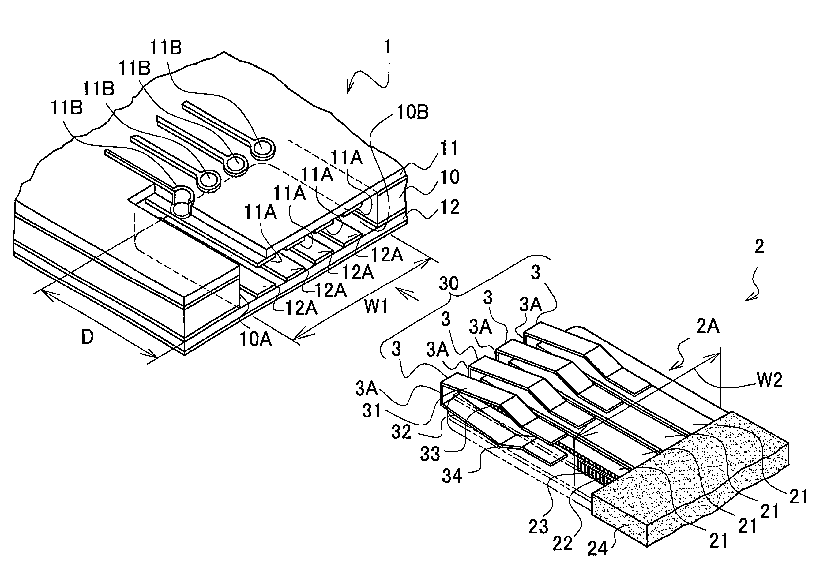
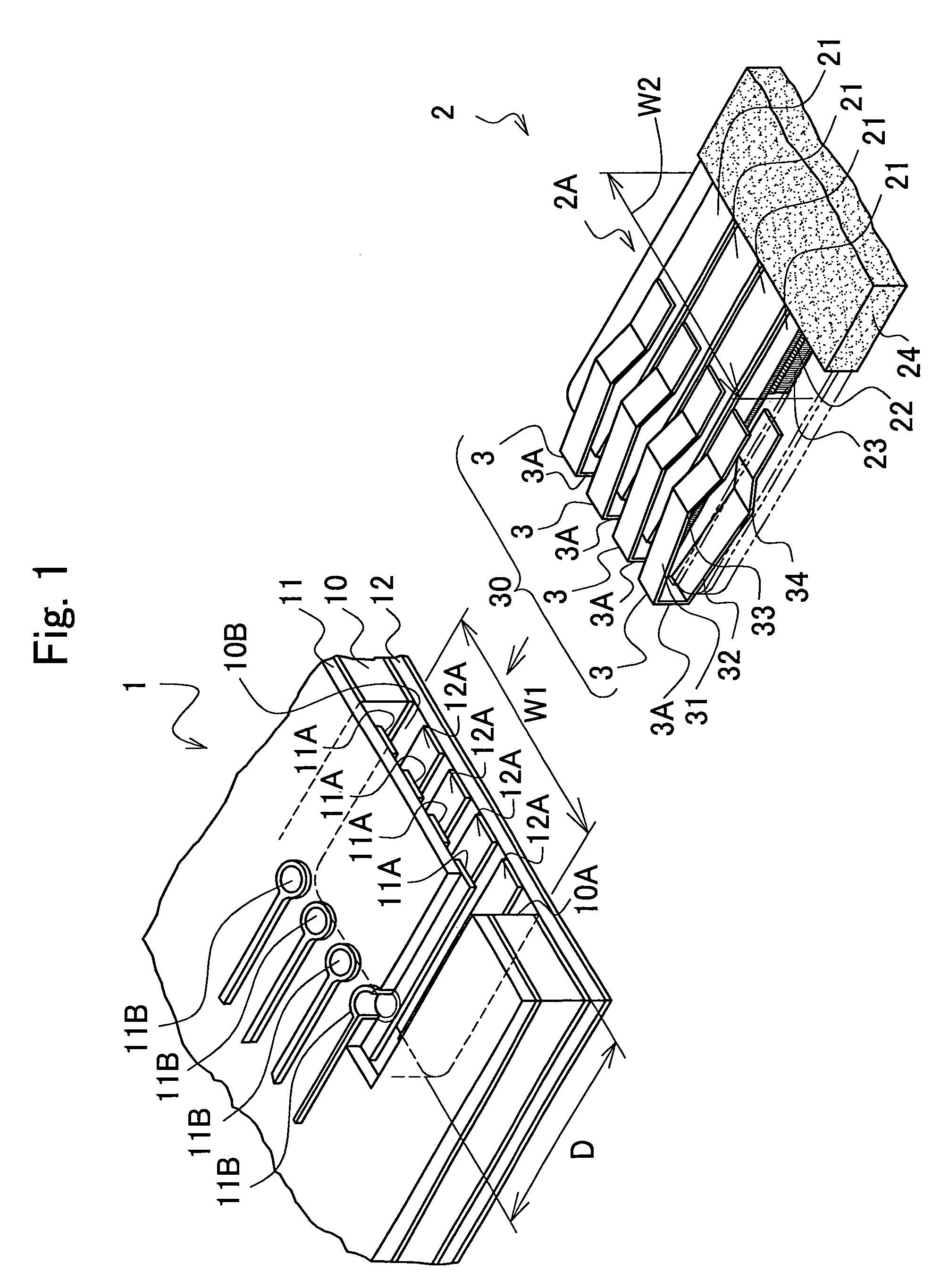
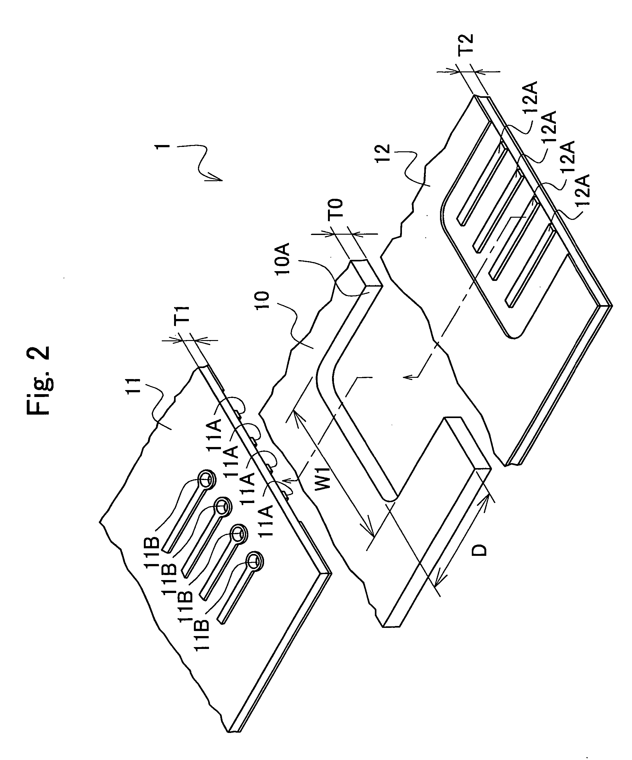
[0065]FIG. 1 is a perspective view showing a FPC 2 and a printed wiring board 1 according to a first embodiment of the present invention.

[0066] The FPC 2 includes an elongated substrate 22, a reinforcing plate 23 adhered onto the lower face of the substrate 22, and plural electro-conductive portions 21 which are layered on the upper surface of the substrate 22 and extend in an axial direction of the substrate 22.

[0067] While the FPC 2 is coated with a polyimide film 24, top end portion thereof is exposed, thereby forming an exposed electro-conductive portion 2A having a width W2.

[0068] The substrate 22 is formed of a material having insulating capabilities, e.g., a thin polyimide film.

[0069] The electro-conductive portions 21 are formed of a favorable material having electro conductivity and formability, and are subjected to nickel plating.

[0070] Furthermore, a dual in-line contact member 30 is fixed to the top end portion of the FPC 2. The dual in-line contact member 30 includ...

second embodiment

[0092] With the present embodiment, a dual in-line contact member 30A has a different configuration from that of the first embodiment.

[0093]FIG. 4 is a perspective view of the FPC 2 according to the second embodiment of the present invention.

[0094] The dual in-line contact member 30A includes a first header 39 holding the main bodies 3A of the first contact members 3 in a state in which the first contact members 3 are arrayed. The first header 39 is formed of synthetic resin and is formed by molding, together with the first contact members 3.

[0095] With the present embodiment, the plural first contact members 3 are arrayed with sufficient precision so that the FPC 2 can be connected to the printed wiring board 1 in more reliable surer manner.

[0096] Next, a procedure for inserting the FPC 2 to the printed wiring board 1 will be described with reference to FIG. 5.

[0097] When the top end portion of the FPC 2 is inserted into the insertion opening 10B of the printed wiring board 1,...

third embodiment

[0098] The present embodiment has generally the same configuration as that of the first embodiment, except for a first adapting connector 5 fixed to the top end portion of the FPC 2 instead of the dual in-line contact member 30.

[0099]FIG. 6 is a perspective view of the FPC 2 and the printed wiring board 1 according to the present embodiment.

[0100] In the top end portion of the FPC 2, the first adapting connector 5 which includes plural elastically deformable second contact members 4 and a first housing 5A holding the second contact members 4 is fixed. Each second contact member 4 includes a main body 4A contacting with the top end portion of the FPC 2, and a third arm 41 and a fourth arm 42 extending from the main body 4A along the surface of the first housing 5A with pinching the electro-conductive portion 21 therebetween. The fourth arm 42 is bent at a bending portion 4D to protrude outward from the first housing 5A.

[0101] The first housing 5A holds the third arms 41 of the sec...


PUM


Abstract

A connecting structure is for a printed wiring board to be electrically connected to a FPC. The FPC includes a substrate and electro-conductive portions. The printed wiring board includes an insertion opening provided on an edge surface thereof, and line connecting terminals formed on an inner wall face of the insertion opening. A dual in-line contact member including first contact members is fixed to the top end portion of the FPC. Each first contact member includes a main body, and a first arm and a second arm extending from the main body generally in parallel to each other. Furthermore, the first arm and the second arm are bent at bent portions so as to form curves protruding away from each other. With the present embodiment, at least one of the first arm and the second arm press the corresponding line connecting terminal provided within the insertion opening at the bent portion thereof by inserting the FPC to the insertion opening of the printed wiring board. Thus, the FPC is connected to the edge surface of the printed wiring board. This improves the freedom from the perspective of design of the wiring pattern as well as allowing mounting of circuit components with high circuit density.

Description

FIELD OF THE INVENTION [0001] The present invention relates to a connection structure for a printed wiring board. More particularly, the present invention relates to a connection structure for a printed wiring board for electrically connecting a FPC (Flexible Printed Circuit) and a printed wiring board formed by stacking plural plate members. RELATED ART [0002] Modules of electronic parts and printed wiring boards are mounted in electronic devices. Conventionally, FPCs, or Flexible Flat Cables, have been used to connect these printed wiring boards and modules of electronic parts. [0003] Here, a printed wiring board includes a base plate having an insulating substrate and a wiring pattern formed on this substrate, and circuit elements, such as ICs and connectors, which are connected to the wiring pattern on the base plate. ZIF (Zero Insertion Force)-type connectors which enable FPCs to be inserted and removed with little force are connectors used as circuit elements mounted on printe...

Claims


Application Information

Patent Timeline
Patent Type & Authority Applications(United States)
IPC IPC(8): H05K1/00H01R13/03H01R24/00H05K1/14H05K3/36H05K3/46
CPCH05K3/365H01R12/728H05K2201/09163H05K1/117H05K2201/10189H05K2201/10265
Inventor UCHIDA, SHINJINAKAI, YOSHIYUKIINOUE, TADASHI
Owner JST MFG CO LTD
Why Eureka
Try Eureka