
MIS capacitor and method of formation

a capacitor and capacitor technology, applied in the field of integrated circuits, can solve the problems of increasing the packing density of cell capacitors at the expense of the available cell area, difficulty in providing sufficient capacitance using conventional stacked capacitor structures, and technical difficulties associated with these materials, so as to improve the cell capacitance and leakage, reduce leakage current, and high capacitance

Inactive Publication Date: 2006-11-02
ROUND ROCK RES LLC
View PDF26 Cites 1 Cited by
  • Summary
  • Abstract
  • Description
  • Claims
  • Application Information

AI Technical Summary

Benefits of technology

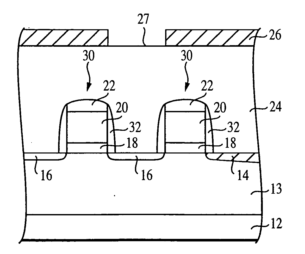
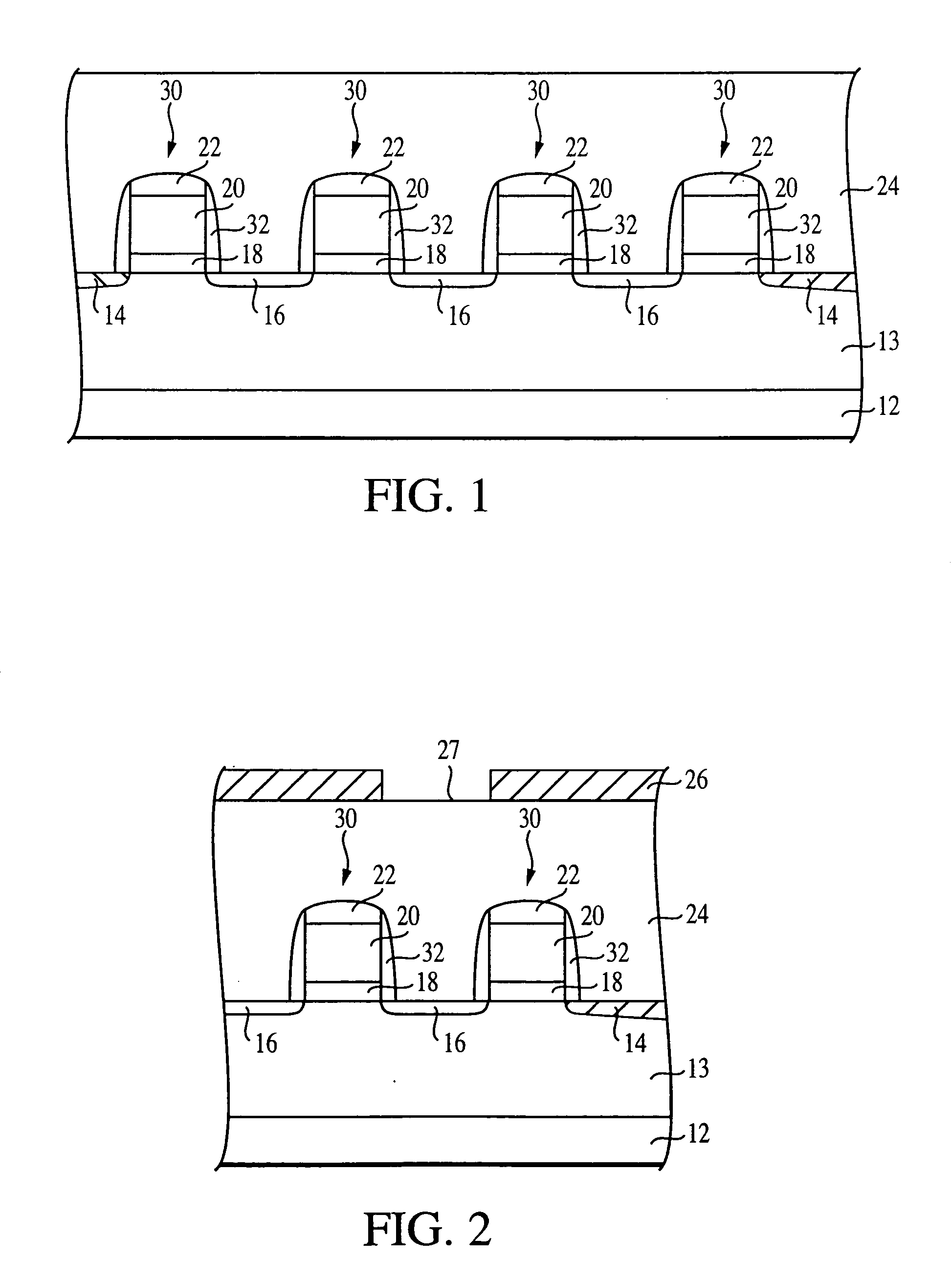
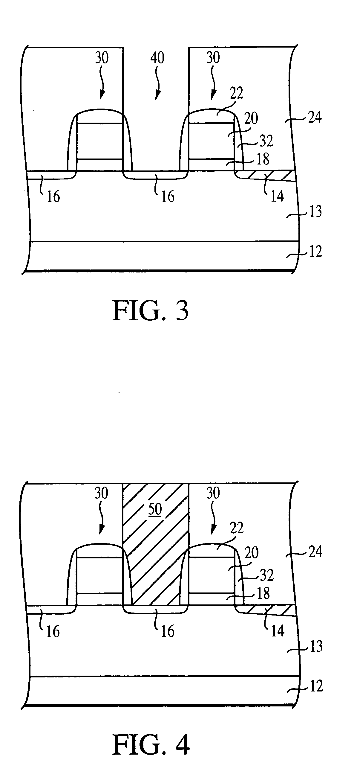
[0008] The present invention provides an MIS capacitor and a method of forming an MIS capacitor with low leakage and high capacitance.
[0010] The present invention also provides a method of forming an MIS capacitor with reduced leakage current and high capacitance. A layer of hemispherical grained polysilicon (HSG) is formed as a lower electrode. After its formation and prior to the dielectric formation, the layer of hemispherical grained polysilicon (HSG) may be subsequently subjected to a nitridization or an anneal process to passivate the HSG surface and improve the cell capacitance and the leakage. A dielectric layer comprising aluminum oxide (Al2O3), or a dielectric composite stack comprising a plurality of interleaved layers of Al2O3 and other dielectric oxides, is formed over the layer of hemispherical grained polysilicon (HSG) by atomic layer deposition (ALD), for example. The dielectric layer or the dielectric composite stack is optionally subjected to a post-dielectric deposition treatment, for example, a nitridization or an anneal treatment, to further reduce leakage and increase the dielectric stability. An upper electrode of metal nitride material is formed over the dielectric layer or the dielectric composite stack by a deposition process or by an atomic layer deposition (ALD) method.

Problems solved by technology

Nevertheless, in the trend to higher memory capacity, the packing density of cell capacitors has increased at the expense of available cell area.
In such limited areas, it is difficult to provide sufficient capacitance using conventional stacked capacitor structures.
Although these materials have a high dielectric constant and low leakage currents, there are some technical difficulties associated with these materials.
One problem with incorporating these materials into current DRAM cell designs is their chemical reactivity with the polycrystalline silicon (polysilicon or “poly”) that conventionally forms a capacitor electrode of a metal-insulator-semiconductor (MIS) capacitor.
The oxide is undesirable because it has a much lower dielectric constant compared to that of PZT / BST, and adds in series to the capacitance of the PZT / BST, thus drastically lowering the total capacitance of the capacitor.
Thus, even a thin native oxide layer present on the electrode results in a large degradation in capacitance.

Method used


Image

  • MIS capacitor and method of formation
  • MIS capacitor and method of formation
  • MIS capacitor and method of formation

Examples


first embodiment

[0087] Under a third set of experiments, a first Al2O3 MIS capacitor was formed on a semiconductor wafer according to the present invention. The first Al2O3 MIS capacitor was fabricated with a lower electrode of CVD hemispherical grained polysilicon of about 400 Angstroms thick, an ALD Al2O3 dielectric layer of about 55 Angstroms thick, and an upper electrode of CVD titanium nitride of about 200 Angstroms thick.

[0088] The ALD Al2O3 dielectric layer of the first Al2O3 MIS capacitor was formed by atomic layer deposition using trimetyl-aluminum (TMA) as an aluminum source precursor and water. The titanium nitride upper electrode was formed by chemical vapor deposition, employing TiCl4 (titanium tetrachloride) as precursor and ammonia (NH3) as nitrogen source.

[0089] A third group of measurements for the capacitance and leakage current of the first Al2O3 MIS capacitor described above was conducted from various die locations across the wafer. The capacitance measurements were conducted a...

second embodiment

[0091] Under a fourth set of experiments, a second Al2O3 MIS capacitor was formed on a semiconductor wafer according to the present invention. The second Al2O3 MIS capacitor was fabricated with a lower electrode of CVD deposited hemispherical grained polysilicon of about 400 Angstroms thick, an ALD Al2O3 dielectric layer of about 55 Angstroms thick subjected to a post-Al2O3 deposition treatment, and an upper electrode of CVD titanium nitride of about 200 Angstroms thick.

[0092] The ALD Al2O3 dielectric layer of the second Al2O3 MIS capacitor was formed by atomic layer deposition using trimetyl-aluminum (TMA) as an aluminum source precursor and water. The titanium nitride upper electrode was formed by chemical vapor deposition, employing TiCl4 (titanium tetrachloride) as precursor and ammonia (NH3) as a nitrogen source.

[0093] Prior to the formation of the ALD Al2O3 dielectric layer, the lower HSG electrode of the second Al2O3 MIS capacitor was subjected to the following sequence of t...

third embodiment

[0096] Under a fifth set of experiments, a third Al2O3 MIS capacitor was formed on a semiconductor wafer according to the present invention. The third Al2O3 MIS capacitor was fabricated with a lower electrode of CVD deposited hemispherical grained polysilicon of about 400 Angstroms thick, an ALD Al2O3 dielectric layer of about 50 Angstroms thick and subjected to a reoxidation treatment, and an upper electrode of CVD titanium nitride of about 200 Angstroms thick.

[0097] The ALD Al2O3 dielectric layer of the third Al2O3 MIS capacitor was formed by atomic layer deposition using trimethyl-aluminum (TMA) as an aluminum source precursor and water. Subsequent to its formation, the ALD Al2O3 dielectric layer of the third Al2O3 MIS capacitor was subjected to a post-deposition oxidation treatment. This way, the ALD Al2O3 dielectric layer underwent an oxidizing ambient under an ozone treatment at about 475° C. for about 3 minutes. The titanium nitride upper electrode was formed by chemical vapo...


PUM

PropertyMeasurementUnit
areaaaaaaaaaaa
thicknessaaaaaaaaaa
temperatureaaaaaaaaaa

Abstract

An MIS capacitor with low leakage and high capacitance is disclosed. A layer of hemispherical grained polysilicon (HSG) is formed as a lower electrode. Prior to the dielectric formation, the hemispherical grained polysilicon layer may be optionally subjected to a nitridization or anneal process. A dielectric layer of aluminum oxide (Al2O3), or a composite stack of interleaved layers of aluminum oxide and other metal oxide dielectric materials, is fabricated over the hemispherical grained polysilicon layer and after the optional nitridization or anneal process. The dielectric layer of aluminum oxide (Al2O3) or the aluminum oxide composite stack may be optionally subjected to a post-deposition treatment to further increase the capacitance and decrease the leakage current. A metal nitride upper electrode is formed over the dielectric layer or the composite stack by a deposition technique or by atomic layer deposition.

Description

FIELD OF THE INVENTION [0001] The present invention relates to the field of integrated circuits and, in particular, to a novel method of forming capacitor structures. BACKGROUND OF THE INVENTION [0002] A dynamic random access memory (DRAM) cell typically comprises a charge storage capacitor coupled to an access device such as a Metal-Oxide-Semiconductor Field Effect Transistor (MOSFET). The MOSFET functions to apply or remove charge on the capacitor, thus affecting a logical state defined by the stored charge. The amount of charge stored on the capacitor is determined by the capacitance C=εεo A / d, where ε is the dielectric constant of the capacitor dielectric, εo is the vacuum permittivity, A is the electrode (or storage node) area, and d is the interelectrode spacing. The conditions of DRAM operation, such as operating voltage, leakage rate and refresh rate, will in general mandate that a certain minimum charge be stored by the capacitor. [0003] In the continuing trend to higher me...

Claims


Application Information

Patent Timeline
Patent Type & Authority Applications(United States)
IPC IPC(8): H01L29/94H01L21/02H01L21/314H01L21/316H01L21/8242
CPCH01L21/3141H01L21/31604H01L21/31616H01L21/31637H01L29/94H01L27/10852H01L28/55H01L28/84H01L28/91H01L21/31645H01L28/40H10B12/033H01L21/0228H01L21/02263H01L21/02178H01L21/02183H01L21/02181
Inventor BASCERI, CEMDERDERIAN, GARO J.
Owner ROUND ROCK RES LLC
Learn More