Priortizing of nets for coupled noise analysis

a technology of coupled noise and prioritization, applied in the field of signal processing system analysis, can solve problems such as chip failure, circuit damage, and various types of noise, and achieve the effect of reducing the number of chips

Inactive Publication Date: 2006-11-02
IBM CORP
View PDF44 Cites 39 Cited by
  • Summary
  • Abstract
  • Description
  • Claims
  • Application Information

AI Technical Summary

Problems solved by technology

Often, a circuit is affected by various types of noise.
In either case, the underlying assumption in the timing tool that these coupled nets are independent is not necessarily valid.
Typically, many signal coupled noise events, such as cross-talk noise, accumulate to result in chip failure.
For example, in digital chips, excessive cross-talk noise on a victim net can lead to logic failure or chip timing failure.
In this regard, cross-talk noise is the noise induced by the parasitic coupling between on-chip wires.
Each coupled noise event has a certain probability of occurring.
The most pessimistic assumption is that any aggressor net or problem-causing signal will switch, and at the worst possible moment, and in the direction th...

Method used


Image

  • Priortizing of nets for coupled noise analysis
  • Priortizing of nets for coupled noise analysis
  • Priortizing of nets for coupled noise analysis

Examples


Embodiment Construction

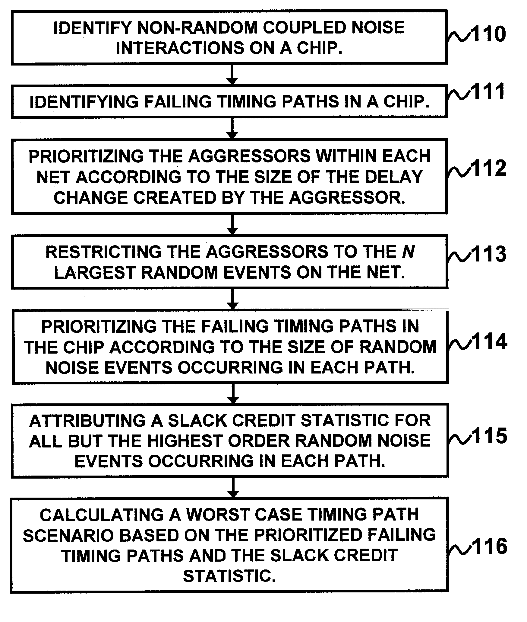
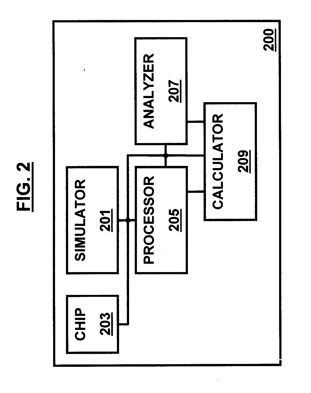
[0020] The embodiments of the invention and the various features and advantageous details thereof are explained more fully with reference to the non-limiting embodiments that are illustrated in the accompanying drawings and detailed in the following description. It should be noted that the features illustrated in the drawings are not necessarily drawn to scale. Descriptions of well-known components and processing techniques are omitted so as to not unnecessarily obscure the embodiments of the invention. The examples used herein are intended merely to facilitate an understanding of ways in which the embodiments of the invention may be practiced and to further enable those of skill in the art to practice the embodiments of the invention. Accordingly, the examples should not be construed as limiting the scope of the embodiments of the invention.

[0021] As mentioned, there remains a need to provide a coupled noise analysis technique which accounts for various parameters presently unacco...


PUM


Abstract

A system and method of performing microelectronic chip timing analysis, wherein the method comprises identifying failing timing paths in a chip; prioritizing the failing timing paths in the chip according to a size of random noise events occurring in each timing path; attributing a slack credit statistic for all but highest order random noise events occurring in each timing path; and calculating a worst case timing path scenario based on the prioritized failing timing paths and the slack credit statistic. Preferably, the random noise events comprise non-clock events. Moreover, the random noise events may comprise victim/aggressor net groups belonging to different regularity groups. Preferably, the size of random noise events comprises coupled noise delta delays due to the random noise events occurring in the chip.

Description

BACKGROUND OF THE INVENTION [0001] 1. Field of the Invention [0002] The embodiments of the invention generally relate to analyzing signal processing systems and, more particularly, to signal timing and noise analysis in electronic circuits. [0003] 2. Description of the Related Art [0004] Full chip timing is typically performed using static timing tools, one net at a time. In this regard, a net is generally defined as a collection of electrical terminals all of which are electrically connected to one another. Static timing analysis is generally an exhaustive technique of analyzing, debugging, and validating the timing performance of a particular chip design. Usually, this is achieved by breaking down the entire design into sets of electrical timing paths. The signal delay on each path in the design is calculated and checked against the known timing parameters for any possible violation. Often, a circuit is affected by various types of noise. A net that is affected by noise is known a...

Claims


Application Information

Patent Timeline
IPC IPC(8): G06F17/50
CPCG06F17/5031G06F30/3312
Inventor FOREMAN, ERIC A.HABITZ, PETER A.SCHAEFFER, GREGORY M.
Owner IBM CORP
Why Eureka
Try Eureka