Nanoimprint lithograph for fabricating nanoadhesive

a nano-adhesive and nano-print technology, applied in the field of nanotechnology, can solve the problems of not meeting the requirements of low production cost and mass production, the current throughput of the technique is too low to be economically practical for mass production, and the mask technology and exposure system are currently rather complex and expensiv

Inactive Publication Date: 2006-11-09
CONTREL TECH CO LTD
View PDF3 Cites 34 Cited by
  • Summary
  • Abstract
  • Description
  • Claims
  • Application Information

AI Technical Summary

Benefits of technology

[0006] The primary objective of the present invention is to provide a low-cost and high-throughput nanoimprint lithography method of fabricating a nanoadhesive.

Problems solved by technology

While the scanning electro beam lithography demonstrated 10-nm resolution, it exposes point by point in a serial manner and thus, the current throughput of the technique is too low to be economically practical for mass production.
The X-ray lithography demonstrated 20-nm resolution in a contact printing mode and has a high throughput, but its mask technology and exposure systems are currently rather complex and expensive.
The lithographies based on scanning proximal probes, demonstrated a resolution of about 10-nm, but were in the early stages of development and failed to meet the requirements of low production cost and mass production, either.

Method used


Image

  • Nanoimprint lithograph for fabricating nanoadhesive
  • Nanoimprint lithograph for fabricating nanoadhesive
  • Nanoimprint lithograph for fabricating nanoadhesive

Examples


Embodiment Construction

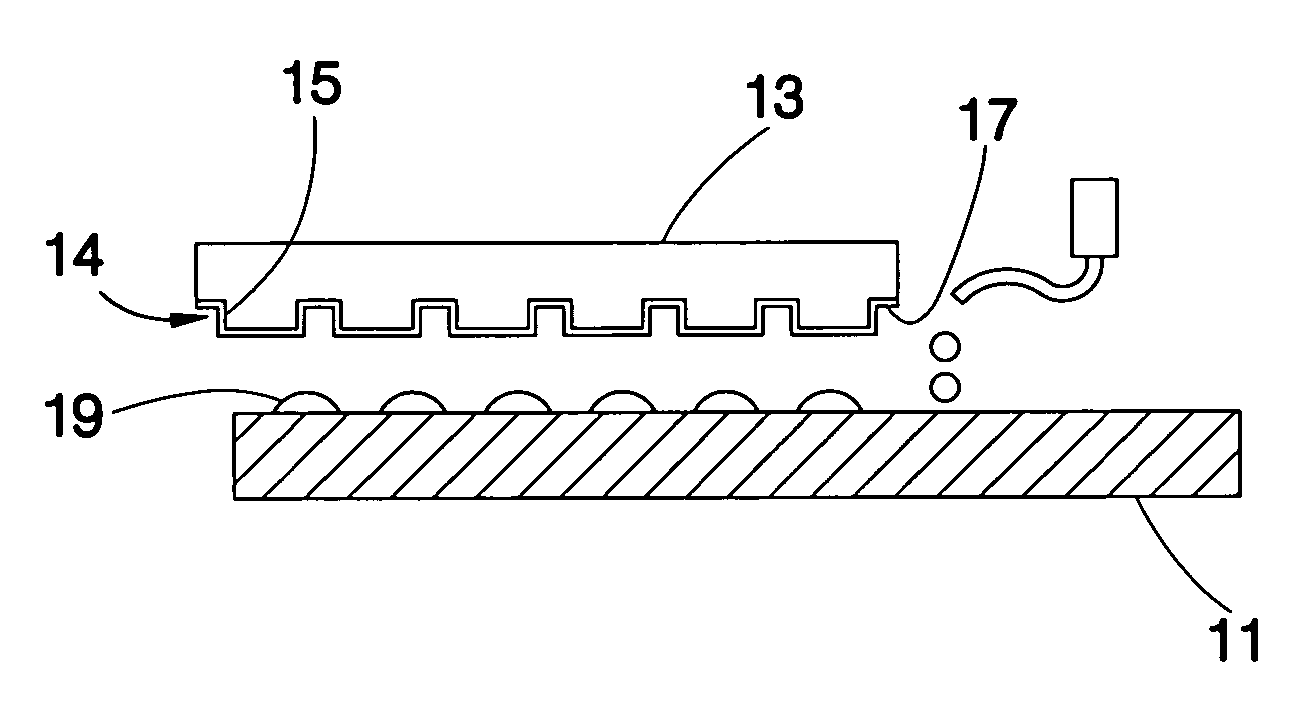
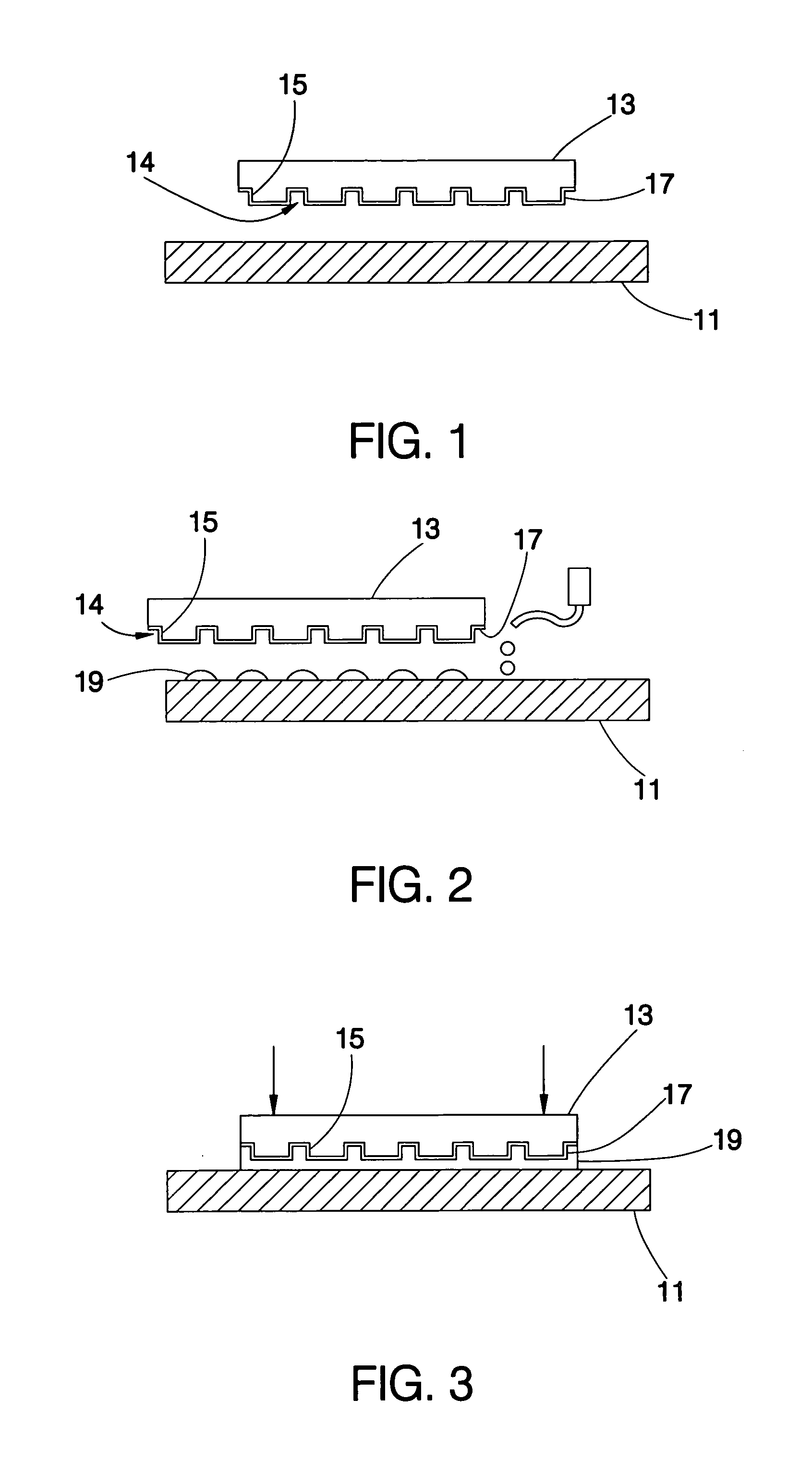
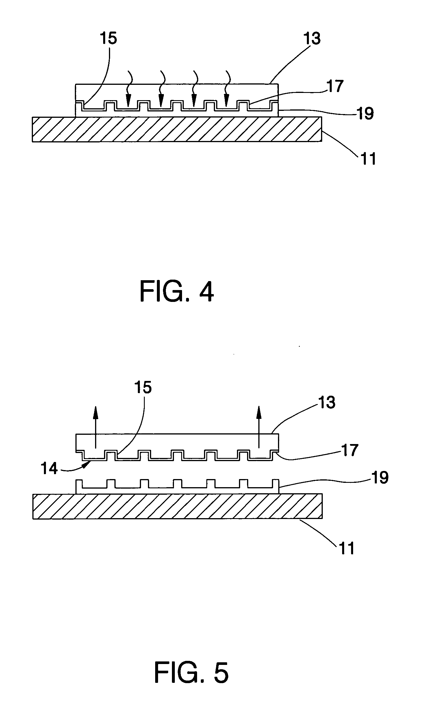
[0027] Referring to FIGS. 1-5, a nanoimprint lithography method of fabricating a nanoadhesive constructed according to a first preferred embodiment of the present invention includes the follows steps.

[0028] (a) Under vacuum environment, prepare a substrate 11 and a mold 13. The mold 13 is transparent plate-like and located over the substrate 11, having an oppressing portion 14 on a bottom side thereof. The oppressing portion 14 has nanometer-scale features 15 on its surface and a mold release agent 17 on the surface of the nanometer-scale features 15, as shown in FIG. 1.

[0029] (b) Coat a liquid resist cast 19 on the substrate 11. The resist cast 19 is a polymer in this embodiment and can be hardened by the irradiation of ultraviolet rays. As shown in FIG. 2, the resist cast 19 like water drops is dropped on the substrate 11 and then coated on the substrate 11 evenly by spinning coating. Since the spinning coating is known as the prior art, no further discussion of this process is ...


PUM

PropertyMeasurementUnit
transparentaaaaaaaaaa
solubleaaaaaaaaaa
water-solubleaaaaaaaaaa

Abstract

A nanoimprint lithography method of fabricating a nanoadhesive includes steps of (a) preparing a substrate and a mold under the vacuum environment, wherein at least one of the substrate and the mold is transparent, the mold is located over the substrate and has an oppressing portion having nanometer-scale features and a mold release agent located on the surface of the nanometer-scale features; (b) coating a liquid resist cast on the substrate, wherein the resist cast can be hardened by ultraviolet rays; (c) having the mold is pressed on the substrate to enable the resist cast to fill between the nanometer-scale features and the substrate; (d) irradiating the resist cast by the ultraviolet rays for hardening; and (e) releasing the mold from the substrate to enable the resist cast to produce a contrast pattern thereon corresponding to the nanometer-scale features, wherein the resist cast with the contrast pattern is the nanoadhesive.

Description

BACKGROUND OF THE INVENTION [0001] 1. Field of the Invention [0002] The present invention relates generally to nanotechnology, and more particularly, to low-cost and high-throughput nanoimprint lithography of fabricating a nanoadhesive. [0003] 2. Description of the Related Art [0004] In the field of the nanotechnology, the imprint lithography techniques can meet the requirements of mass production and low production cost. Particularly, the imprint lithography technique with the sub-50-nm line-width is essential for the further manufacturing of semiconductor integrated circuits and the commercialization of electronic, optoelectronic, and magnetic nanodevices. [0005] Numerous relevant technologies are under development, like scanning electro beam lithography (K. C. Beard, T. Qi. M. R. Dawson, B. Wang. C. Li, Nature 368, 604 (1994)), X-ray lithography (M. Godinot and M. Mahboubi, C. R. Acad. Sci. Ser. II Mec. Phys. Chim. Chim. Sci. Terre Univers. 319, 357(1994); M. Godinot, in Anthropo...

Claims


Application Information

Patent Timeline
Patent Type & Authority Applications(United States)
IPC IPC(8): B29C35/08B29C33/76B29C59/02
CPCB29C35/0888B29C43/003B29C43/021B29C43/06B29C2035/0827G03F7/0002B29C2043/3438B29C2043/463B82Y10/00B82Y40/00B29C2043/025B82B3/00C09J11/00
Inventor CHAO, CHIH-YUHSIEH, WEN-JIUNN
Owner CONTREL TECH CO LTD
Why Eureka
Try Eureka