OLED device with improved light output

a light-emitting diode and oled technology, which is applied in the direction of discharge tube/lamp details, organic semiconductor devices, discharge tubes luminescnet screens, etc., can solve the problems of limited current carrying capacity of such electrodes, affecting the light output of oled devices, and limiting the amount of light that can be emitted from organic layers, etc., to achieve increased light output, reduce light absorbance, and increase transparency

Inactive Publication Date: 2006-11-09
EASTMAN KODAK CO
View PDF20 Cites 119 Cited by
  • Summary
  • Abstract
  • Description
  • Claims
  • Application Information

AI Technical Summary

Benefits of technology

[0025] Various embodiments of the present invention have the advantages that by employing an encapsulating layer specifically designed to increase transparency and/or decrease light absorbance in an adjacent electrode, light output from an OLED device may be increased. Various embodiments further enabl

Problems solved by technology

However, the current carrying capacity of such electrodes is limited, thereby limiting the amount of light that can be emitted from the organic layers.
Moreover, metallic layers may create unwanted cavity effects.
In contrast, typically polymeric materials have a moisture permeation rate of approximately 0.1 gm/m2/day and cannot adequately protect the OLED materials without additional moisture blocking layers.
However, as taught in the prior art, such coatings might not be sufficiently conductive or transparent to provide or enable a transparent, conductive electrode.
However, this increases the area of the substrate and cover and is not completely effective.
This approach is less practical for top-emitters, since the desiccants, in that case, need to be highly transparent and uniformly distributed.
While highly light-transmissive electrode materials such as ITO have been proposed for top-emitting devices, ITO does not provide as high a conductivity as may be desired.
However, such microcavity designs require very precise control of layer thicknesses in order to obtain the desired color, and may also create a strong angular dependence on the color of light emitted, especiall

Method used


Image

  • OLED device with improved light output
  • OLED device with improved light output
  • OLED device with improved light output

Examples


Embodiment Construction

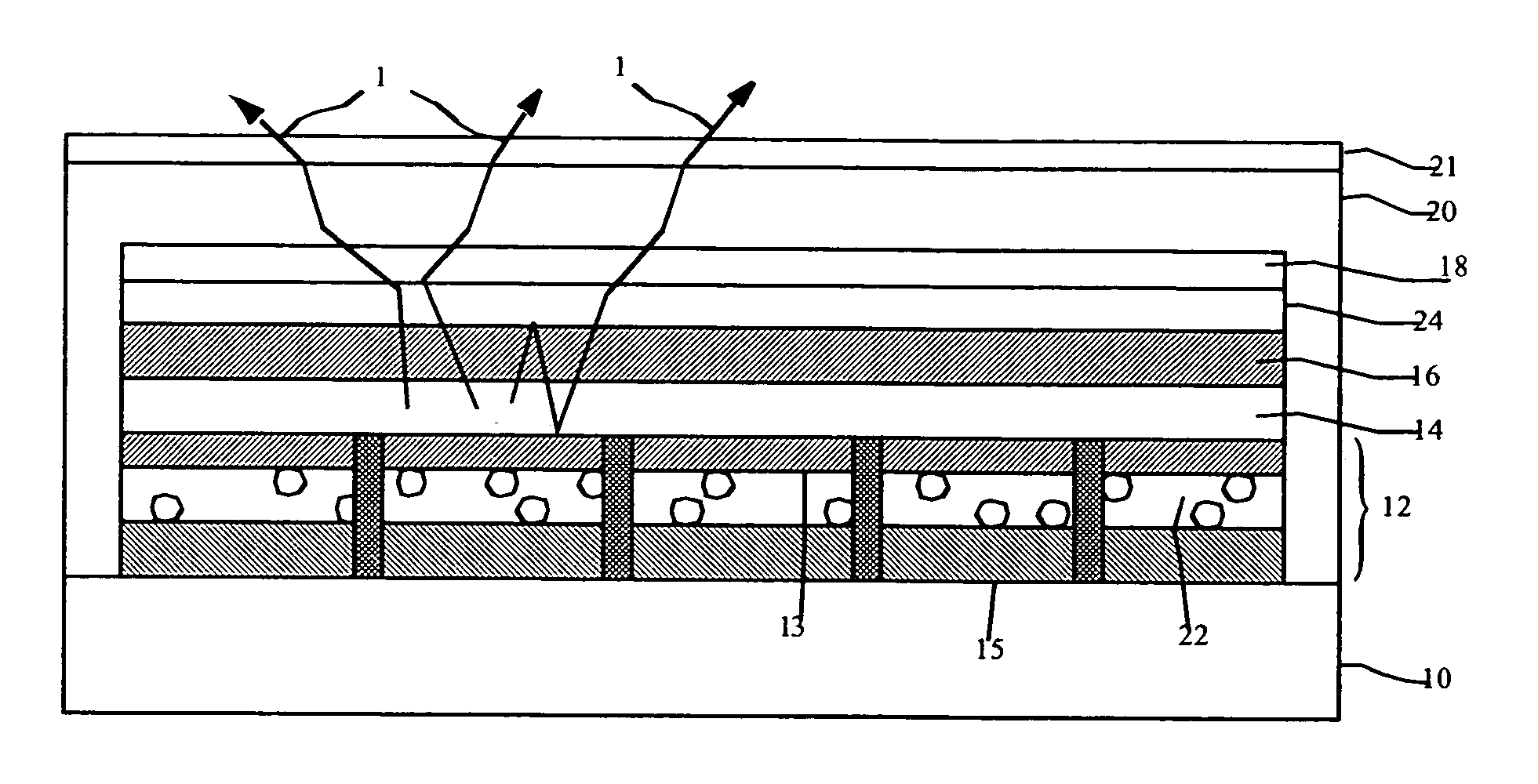
[0036] Referring to FIG. 1, in accordance with one embodiment of the present invention, an organic light-emitting diode (OLED) device comprises a substrate 10; an OLED formed over the substrate 10 comprising a first electrode 12, a partially transparent second electrode 16 through which light from the OLED is emitted, and at least one layer 14 of organic light-emitting material disposed between the first electrode 12 and the partially transparent second electrode 16; an encapsulating layer 24 comprises one or more component layers deposited on the partially transparent second electrode 16, wherein the encapsulating layer 24 and the partially transparent second electrode 16 combined have a transparency greater than the transparency of the partially transparent second electrode 16 in the absence of the encapsulating layer 24, or wherein the encapsulating layer 24 and the partially transparent second electrode 16 combined have an absorbance less than the absorbance of the partially tra...


PUM


Abstract

An organic light-emitting diode (OLED) device is described, comprising: a) a substrate; b) an OLED formed over the substrate comprising a first electrode, a partially transparent second electrode through which light from the OLED is emitted, and at least one layer of organic light-emitting material disposed between the first electrode and partially transparent second electrode; and c) an encapsulating layer deposited on the partially transparent second electrode, wherein the encapsulating layer comprises one or more component layers, and wherein the encapsulating layer and the partially transparent second electrode combined have a transparency greater than the transparency of the partially transparent second electrode in the absence of the encapsulating layer, or wherein the encapsulating layer and the partially transparent second electrode combined have an absorbance less than the absorbance of the partially transparent second electrode in the absence of the encapsulating layer. To provide adequate encapsulation, in accordance with various embodiments of the invention at least one component layer of the encapsulating layer is deposited by atomic layer deposition, or the total thickness of encapsulating layer is at least about 150 nm. In a preferred embodiment, both such features are incorporated.

Description

FIELD OF THE INVENTION [0001] The present invention relates to organic light-emitting diode (OLED) devices and, more particularly, to a method of making an OLED device having improved light output and power distribution through a light-transmissive electrode. BACKGROUND OF THE INVENTION [0002] Organic light-emitting diode (OLED) devices, also referred to as organic electroluminescent (EL) devices, have numerous well-known advantages over other flat-panel display devices currently in the marketplace. Among the potential advantages are brightness of light emission, relatively wide viewing angle, reduced device thickness, and reduced electrical power consumption compared to, for example, liquid crystal displays (LCDs) using backlighting. [0003] Applications of OLED devices include active-matrix image displays, passive-matrix image displays, and area-lighting devices such as, for example, selective desktop lighting. Irrespective of the particular OLED device configuration tailored to th...

Claims


Application Information

Patent Timeline
IPC IPC(8): H05B33/14H01J1/62
CPCH01L51/5234H01L51/5237H01L2251/5315H01L51/5268H01L51/5262H10K50/818H10K50/828H10K50/85H10K50/841H10K50/854H10K2102/3026H10K50/844
Inventor COK, RONALD S.SHORE, JOEL D.
Owner EASTMAN KODAK CO
Why Eureka
Try Eureka