Electro-optical device, color filter substrate and electronic apparatus

a technology of optical devices and substrates, applied in the field of optical devices, color filter substrates and electronic devices, can solve the problems of insufficient display brightness, degrading the saturation of transmissive displays, and unable to achieve sufficient saturation in transmissive displays, so as to improve the brightness of reflective displays, increase the power consumption of backlights, and improve the effect of brightness

Inactive Publication Date: 2006-11-09
138 EAST LCD ADVANCEMENTS LTD
View PDF18 Cites 1 Cited by
  • Summary
  • Abstract
  • Description
  • Claims
  • Application Information

AI Technical Summary

Benefits of technology

[0054] In addition, the coverage area ratio of the colored layer of green color is preferably 30-50%, and the coverage area ratio of the colored layers of red and blue colors is preferably 60-100%. The color reproducibility and the brightness of the reflective display can be improved while ensuring the color reproducibility of the transmissive display by setting the coverage area ratio of green color and the coverage area ratio of red and blue colors in the above ranges. In particular, the coverage area ratio of the colored layer of green color is most preferably 35-45%, and the coverage area ratio of the colored layers of red and blue colors is most preferably 85-100%.
[0055] In addition, the reflection part is preferably disposed on the entire periphery of the aperture. Since the aperture is surrounded by the reflection part in the reflective layer, any area not covered by the colored layer is prevented from being generated in the aperture even when a slight positional deviation is generated between the colored layer and the reflective layer. In particular, the aperture is preferably formed substantially in the center of the reflective layer.
[0056] In addition, the aperture ratio by the aperture with respect to the reflective layer is preferably 30-70%. Generally, if the aperture ratio of the reflective layer is increased, the transmissive display is brightened while the reflective display is darkened, and it is necessary to set the aperture ratio of the reflective layer so that the transmissive display and the reflective display are balanced. More specifically, if the aperture ratio is too small, the illuminance of the backlight must be higher, and the power consumption of the backlight is increased. On the other hand, if the aperture ratio is too large, the reflective display is darkened, and less easily recognized visually. In the present embodiment, the brightness of the reflective display can be ensured by providing an area not overlapping the colored layer on a part of the reflection part, and the transmissive display and the reflective display can be balanced in the range of the large aperture ratio compared with the case of employing a structure with the colored layer overlapping the entire reflective layer, and excellent color quality can be realized in both the transmissive display and the reflective display. When the aperture ratio is below the above range, the power consumption is increased so as to ensure the brightness of the transmissive display, the present embodiment is less easily employed in a portable electronic apparatus such as a cellular phone. If the aperture ratio is above the range, the brightness and the saturation in the reflective display are less easily consistent, and the color quality in the reflective display is less easily ensured.

Problems solved by technology

In addition, a problem occurs in that saturation in the transmissive display is degraded with respect to saturation of the reflective display.
This means that, in the reflective display, display brightness is generally insufficient, and display brightness must be ensured by setting the light transmittance ratio of the color filter 112 to be high.
However, in this configuration, sufficient saturation cannot be obtained in the transmissive display.
A problem of sense of incongruity thus occurs.

Method used


Image

  • Electro-optical device, color filter substrate and electronic apparatus
  • Electro-optical device, color filter substrate and electronic apparatus
  • Electro-optical device, color filter substrate and electronic apparatus

Examples


first embodiment

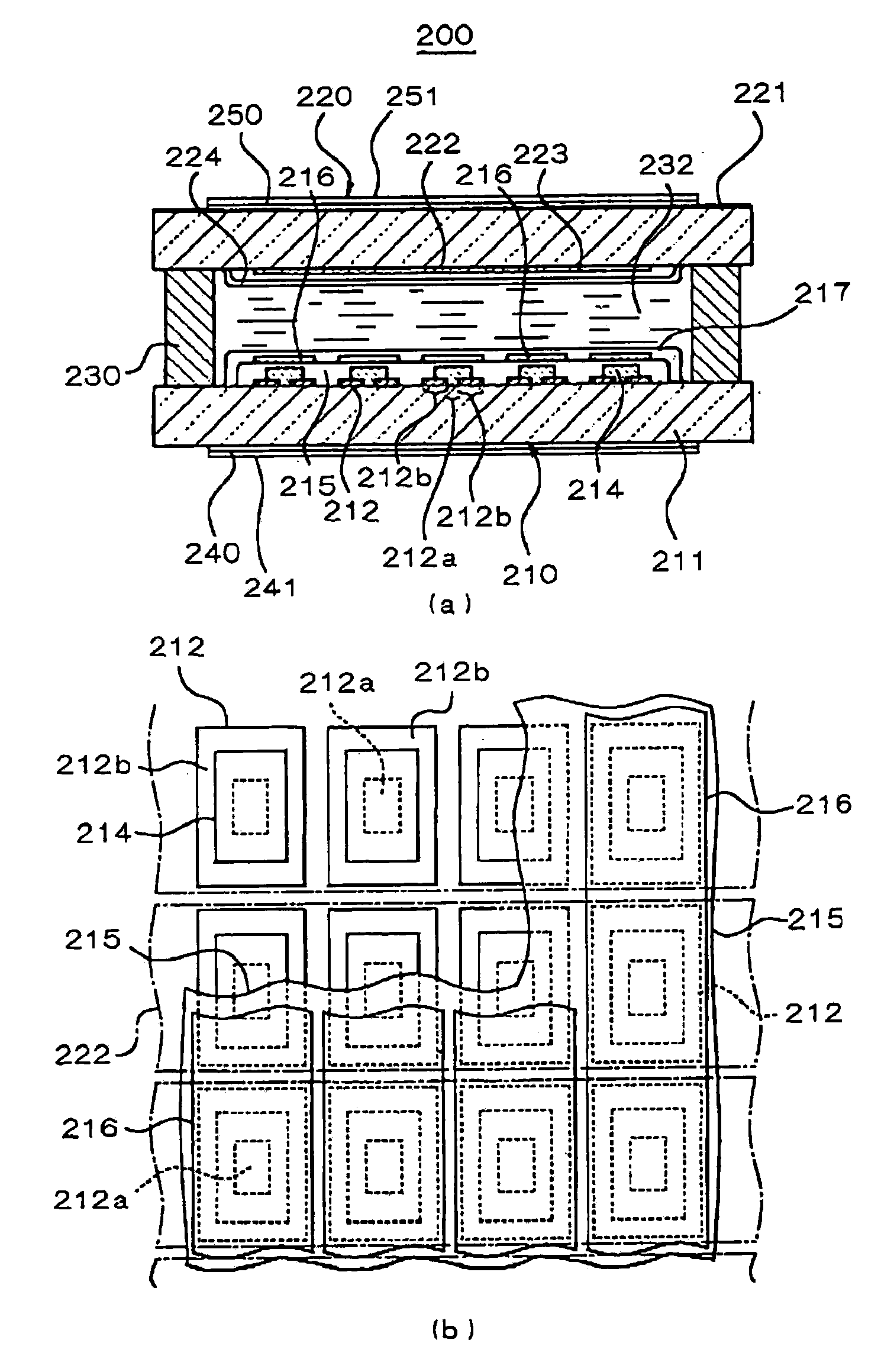
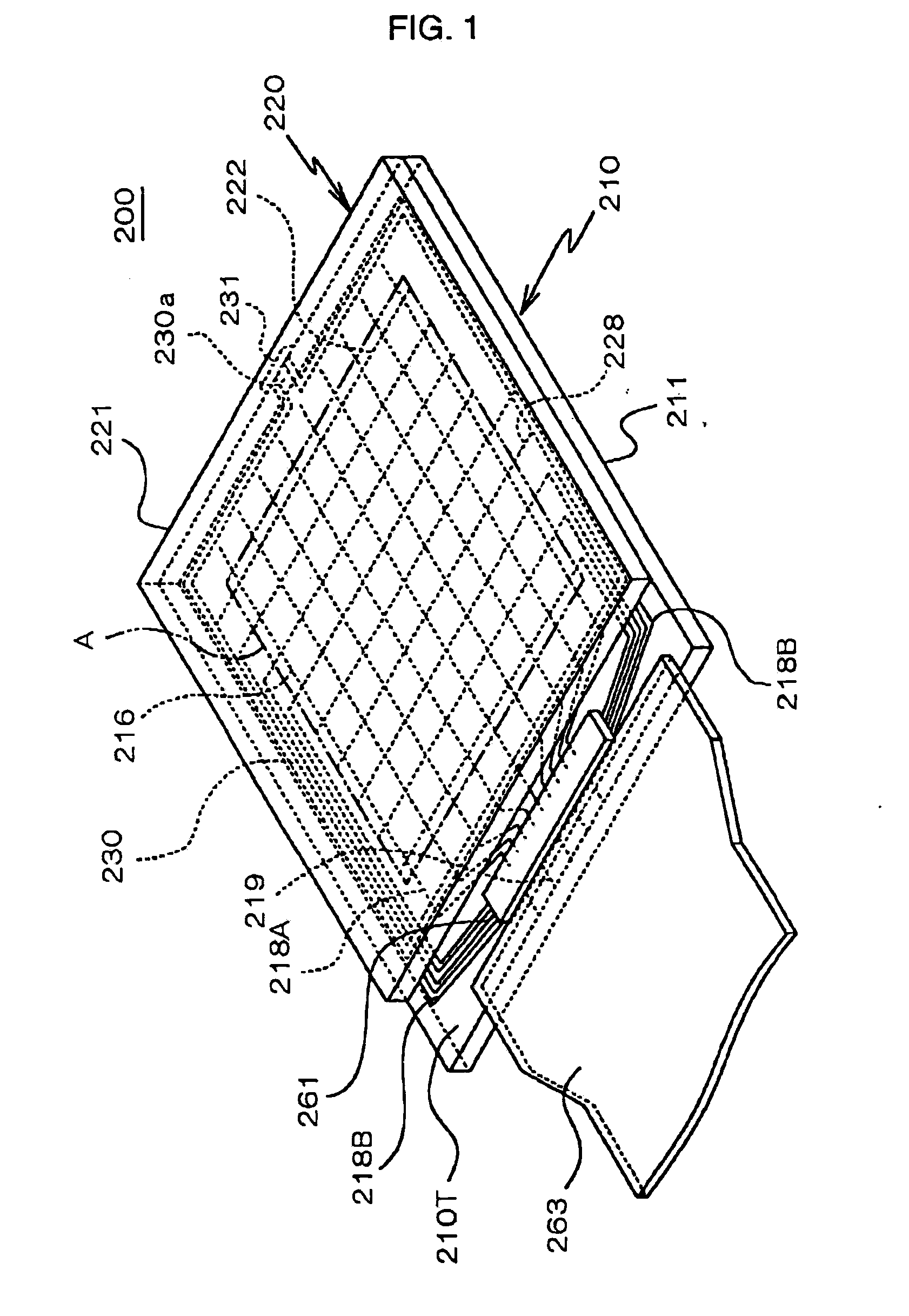
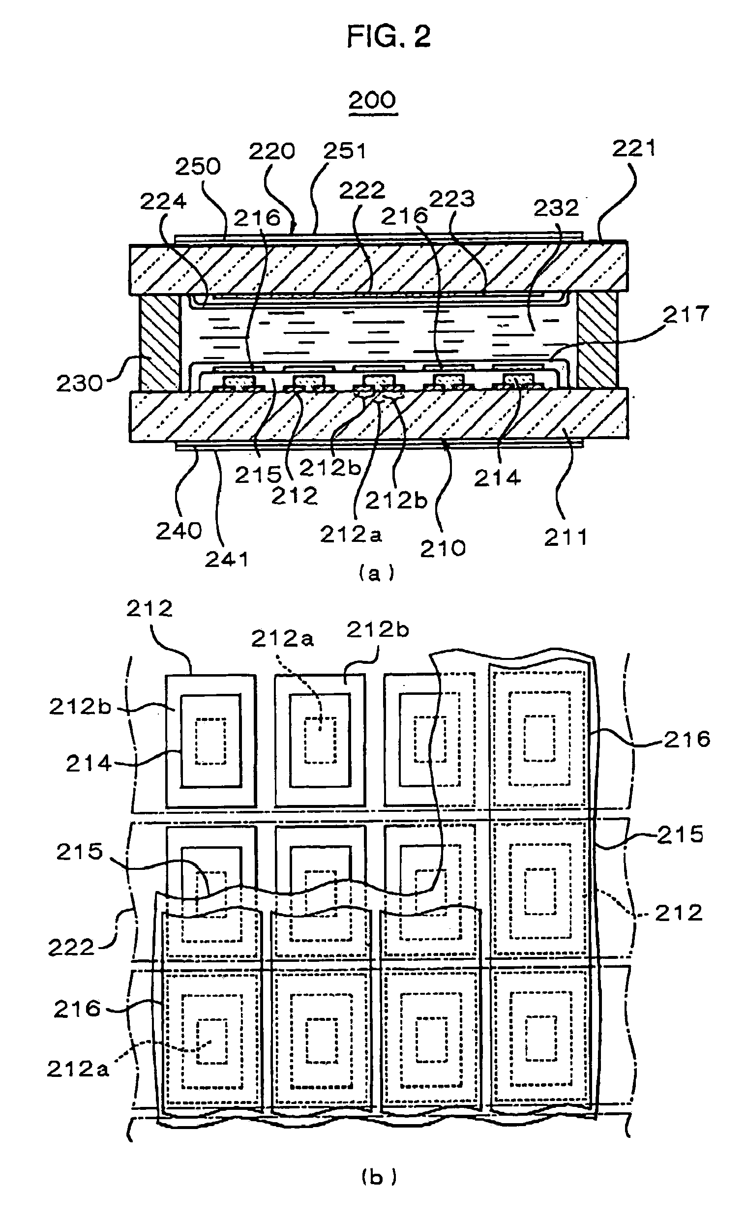
[0078]FIG. 1 is a schematic perspective view showing the appearance of a liquid crystal display panel 200 constituting an electro-optical device according to a first embodiment of the present invention, FIG. 2(a) is a schematic sectional view of the liquid crystal display panel 200, and FIG. 2(b) is a partially enlarged plan view of a color filter 210 constituting the liquid crystal display panel 200.

[0079] This electro-optical device has an illumination device such as a backlight and a front light (not shown), a casing, etc. as necessary on the liquid crystal display panel 200 having a so-called transflective passive matrix structure.

[0080] As shown in FIG. 1, the liquid crystal display panel 200 has a cell structure in which a color filter substrate 210 basically consisting of a transparent first substrate 211 formed of a glass plate or a synthetic resin plate, and a facing substrate 220 basically comprising a similar second substrate 221 facing thereto are affixed to each other...

second embodiment

[0097] Next, description will be made on a second embodiment of the present invention with reference to FIGS. 3(a) and 3(b). The liquid crystal display panel 300 of the present embodiment comprises a first substrate 311, a second substrate 321, a colored layer 314, a surface protection layer 315, a transparent electrode 316, an alignment layer 317, a transparent electrode 322, a hard protection film 323, an alignment layer 324, a sealing member 330, a liquid crystal 332, retardation films 340 and 350, and polarizers 341 and 351 similarly to the first embodiment described above, and description of these components is omitted.

[0098] In the liquid crystal display panel 300 of the present embodiment, the reflective layer 312 is integrally formed in a substantially overall manner in the liquid crystal display area, and an aperture 312 is disposed for each pixel. A part other than the aperture 312a out of the reflective layer 312 forms a reflection part 312b for substantially reflecting ...

third embodiment

[0100] Next, description will be made on a third embodiment in accordance with the present invention with reference to FIGS. 4(a) and 4(b). A liquid crystal display panel 400 of the present embodiment comprises a first substrate 411, a second substrate 421, a reflective layer 412 having an aperture 412a and a reflection part 412b, a transparent electrode 416, an alignment layer 417, a transparent electrode 422, an alignment layer 423, sealing members 430, a liquid crystal 432, retardation films 440 and 450, and polarizer 441 and 451, and the description on these components will be omitted.

[0101] In the present embodiment, as shown in FIG. 4(a), a color filter is formed not on a first substrate 421 with a reflective layer 412 formed thereon, but on a second substrate 421. More specifically, a color filter 424 is formed on the second substrate 421 for each pixel, and a black shielding film 424BM similar to that in the second embodiment is formed in the area between pixels. A transpar...


PUM

PropertyMeasurementUnit
wavelengthaaaaaaaaaa
areaaaaaaaaaaa
coloraaaaaaaaaa

Abstract

A reflective layer 212 having an aperture 212a for each pixel is formed on a first substrate 211, and a colored layer 214 for constituting a color filter is formed thereon. A surface protection layer 215 is formed on the colored layer 214, and a transparent electrode 216 is formed further thereon. The colored layer 214 is constituted so as to cover the aperture 212a in a two-dimensional direction, but overlaps only a part of a reflection surface in the pixel in a two-dimensional direction.

Description

CROSS-REFERENCE TO RELATED APPLICATIONS [0001] This application is a divisional of U.S. patent application Ser. No. 10 / 206,784 filed on Jul. 26, 2002, which claims the benefit of Japanese Patent Application No. 2001-228447 filed Jul. 27, 2001 and Japanese Patent Application No. 2002-188602 filed Jun. 27, 2002. The disclosures of the above applications are incorporated herein by reference.BACKGROUND OF THE INVENTION [0002] 1. Technical Field of the Invention [0003] The present invention relates to an electro-optical device, a color filter substrate and an electronic apparatus, and more specifically, it relates to a technology suitable for a structure of a color electro-optical device having a reflective layer. [0004] 2. Description of the Related Art [0005] Transflective display type liquid crystal display panels capable of visually recognizing reflective display utilizing the external light and transmissive display utilizing illumination light such as a backlight have been known. Th...

Claims


Application Information

Patent Timeline
Patent Type & Authority Applications(United States)
IPC IPC(8): G02F1/1335G02B5/00G02B5/20G09F9/30G09F9/35
CPCG02F1/133555G02F1/133514G02F1/1335
Inventor TAKIZAWA, KEIJIOTAGIRI, YOSHIHIRO
Owner 138 EAST LCD ADVANCEMENTS LTD
Why Eureka
Try Eureka