Apparatus and method for waveguide to microstrip transition having a reduced scale backshort

a waveguide and microstrip technology, applied in electrical apparatus, multiple-port networks, resonances, etc., can solve the problems of difficult to properly realize matching circuits, difficult to match open-ended waveguides, and constraint that the backshort b>1514/b> has a considerable length, so as to reduce the scale

Active Publication Date: 2006-11-16
FURUNO ELECTRIC CO LTD
View PDF10 Cites 27 Cited by
  • Summary
  • Abstract
  • Description
  • Claims
  • Application Information

AI Technical Summary

Benefits of technology

[0013] Accordingly, embodiments of the present invention are directed to a transition between a waveguide and a microstrip which may reduce their scale and address the challenges associated with the related art.

Problems solved by technology

One potential issue with conventional transition 1500 is that it may be difficult to match the impedance between open-ended waveguide 1510 and microstrip 1516 given the large relative difference in the magnitude of their respective impedances.
Given the differences in impedances, and the interaction of EM fields within the waveguides, it may be difficult to properly realize matching circuit 1614, which may utilize sophisticated three-dimensional circuit design.
Another potential issue with conventional transition 1500 may be the constraint that backshort 1514 has a considerable length which typically is greater than λ / 4.

Method used


Image

  • Apparatus and method for waveguide to microstrip transition having a reduced scale backshort
  • Apparatus and method for waveguide to microstrip transition having a reduced scale backshort
  • Apparatus and method for waveguide to microstrip transition having a reduced scale backshort

Examples


first embodiment

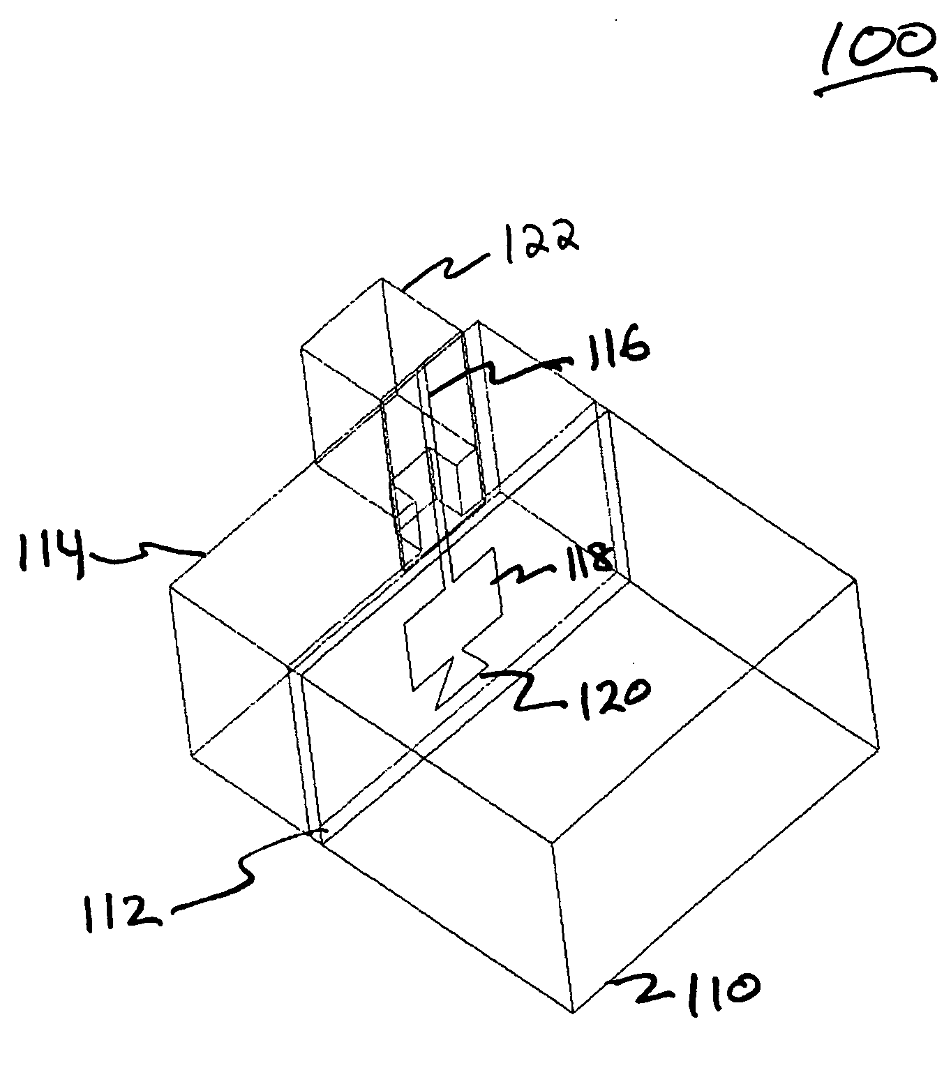
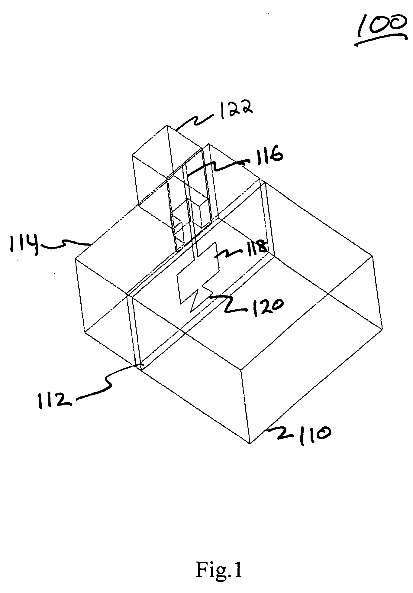
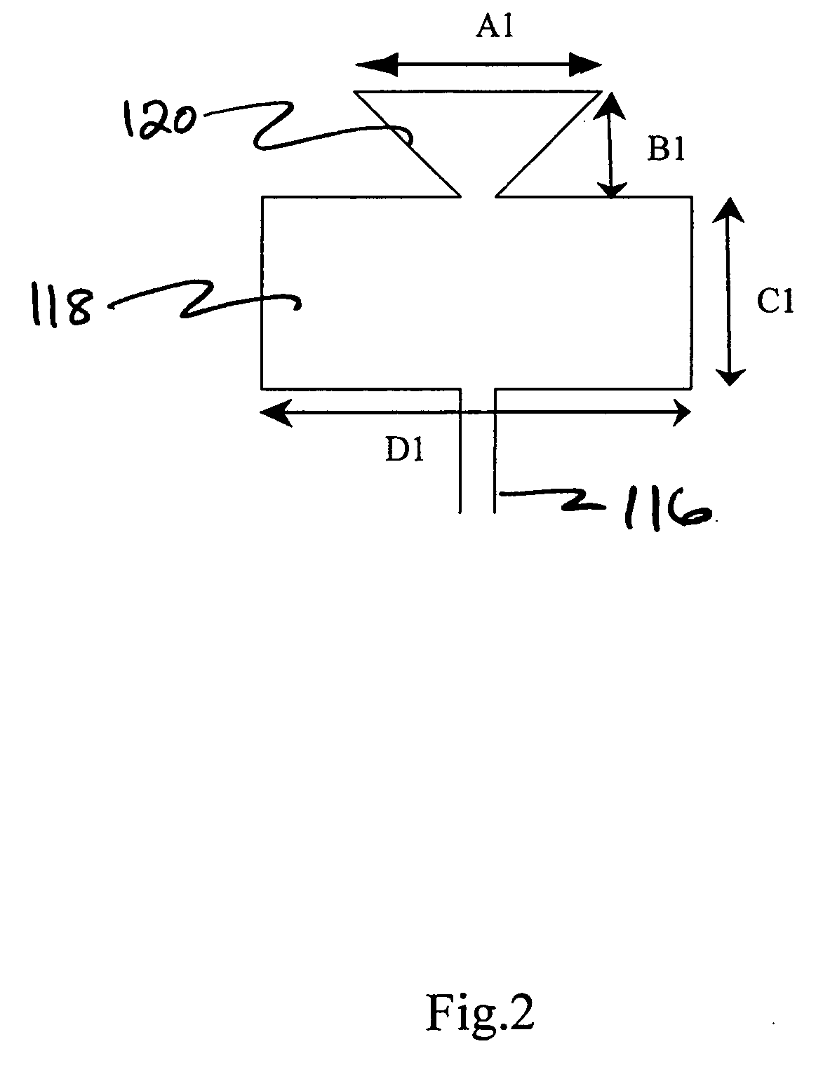
[0036]FIG. 1 shows a transition 100, passing electromagnetic (EM) waves between a waveguide and microstrip consistent with the present invention. Transition 100 includes an open-ended waveguide 110, a substrate 112, a backshort 114 having reduced scale, a microstrip 116, a resonator 118, and a conductor pad 120.

[0037] As used herein, the expression “reduced scale” may refer to a reduction is the size of the backshort 114 in any dimension; and includes reductions of size in the dimension of EM wave propagation. For example, reduced scale backshort 114 may include a backshort having a dimension in the direction of EM wave propagation which may be less than or equal to a quarter wavelength (λ / 4) of the EM wave. It should be noted that the reduced scale backshort 114 dimensions may be arbitrary and are not limited only to integer fractions of a wavelength (λ).

[0038] Embodiments of the invention typically may utilize EM waves having frequencies in the microwave region. However, the EM w...

second embodiment

[0058]FIG. 6 shows the results of an exemplary simulation estimating the frequency performance associated with the invention shown in FIG. 5. This graph shows the magnitude of the impedance associated with parameters of a scattering matrix, S11 and S21, over a frequency range of 8.5 GHz to 10.5 GHz. S11 may be associated with the magnitude of a reflecting EM wave, and S21 may be associated with the magnitude of a EM wave passing through transition 500. As before, S11 and S21 represent values that can be measured between the edge of open-ended waveguide 110 and the edge of microstrip 116.

[0059] As can be seen from FIG. 6, the curve simulating the magnitude S11 shows a “dip” around 9 GHz where EM energy associated with desirable frequencies tends to not be reflected. In this embodiment, reflections may be attenuated approximately −15 dB around 9 GHz. While this attenuation level may be less than that shown in FIG. 3, it may be sufficient for applications where transition 500 can be us...

sixth embodiment

[0069]FIG. 12 shows the results of an exemplary simulation estimating the frequency performance associated with the invention. This graph shows the magnitude of the impedance associated with parameters of a scattering matrix, S11 and S21, over a frequency range of 8.5 GHz to 10.5 GHz. S11 may be associated with the magnitude of a reflecting EM wave, and S21 may be associated with the magnitude of a EM wave passing through transition 1000. As before, S11 and S21 represent values that can be measured between the edge of open-ended waveguide 110 and the edge of microstrip 116.

[0070] As can be seen from FIG. 12, the curve simulating the magnitude S11 shows a steep “dip” around 9 GHz where EM energy associated with desirable frequencies tend to not be reflected. This embodiment has the advantage of not only attenuating reflections by approximately a steep −45 dB around 9 GHz, but also reflects undesirable frequencies as shown by the “bump” is S11 at 10 GHz. The curve simulated the magnit...


PUM


Abstract

Methods and apparatuses are directed to a transition between a waveguide and a microstrip. One embodiment features an open-ended waveguide having an exposed side at a distal end, a substrate coupled to the open-ended waveguide at a proximate end, a resonator coupled to the substrate, a microstrip line electromagnetically coupled to the resonator, and a backshort coupled to the substrate. Another embodiment features receiving an electromagnetic wave, collecting an incident portion of the received electromagnetic wave, generating first wave having a resonance at a predetermined frequency using the incident portion of the received electromagnetic wave, reflecting a portion of the received electromagnetic wave off of a reduced scale backshort, back towards a collector, generating a second wave having a resonance at a predetermined frequency using the reflected portion of the received electromagnetic wave, and combining the first wave and the second wave in phase.

Description

CROSS-REFERENCE TO RELATED APPLICATION [0001] This non-provisional application claims priority under 35 U.S.C. §119(e) of U.S. Provisional Application No. 60 / 672,009 filed Apr. 18, 2005, the entire contents thereof are relied upon and are expressly incorporated herein by reference.BACKGROUND OF THE INVENTION [0002] 1. Field of the Invention [0003] Embodiments of the present invention generally relate to Microwave Integrated Circuits (MIC) and monolithic devices, and more specifically, to transitions between waveguides and microstrips for devices operating in microwave and millimeter wave frequencies. [0004] 2. Description of the Background Art [0005] Conventional techniques have been designed and developed to facilitate efficient transitions between waveguide and microstrip structures. These transitions may be used in a variety of integrated circuit devices which may operate in the RF, microwave, and millimeter wave frequency regimes. The transitions can effectively serve to act as ...

Claims


Application Information

Patent Timeline
Patent Type & Authority Applications(United States)
IPC IPC(8): H01P5/107
CPCH01P5/107
Inventor IIO, KENICHI
Owner FURUNO ELECTRIC CO LTD
Why Eureka
Try Eureka