Eclipse elimination by monitoring the pixel signal level

a technology of pixel signal level and pixel architecture, applied in the field of pixel architecture, can solve problems such as the pixel being susceptible to an eclipse condition

Active Publication Date: 2006-11-16
MICRON TECH INC
View PDF8 Cites 21 Cited by
  • Summary
  • Abstract
  • Description
  • Claims
  • Application Information

AI Technical Summary

Benefits of technology

[0019] Exemplary embodiments of the method and apparatus of the present invention provide an anti-eclipse circuit for an imager. The anti-eclipse circuit permits a pixel to initially output a reset signal, which is sampled-and-held. Subsequently, when the pixel outputs a photo signal, which is also sampled-and-held. While the pixel is outputting the photo signal, the voltage level of the photo signal is monitored to determine wh...

Problems solved by technology

If so, the pixel may be sus...

Method used


Image

  • Eclipse elimination by monitoring the pixel signal level
  • Eclipse elimination by monitoring the pixel signal level
  • Eclipse elimination by monitoring the pixel signal level

Examples


Embodiment Construction

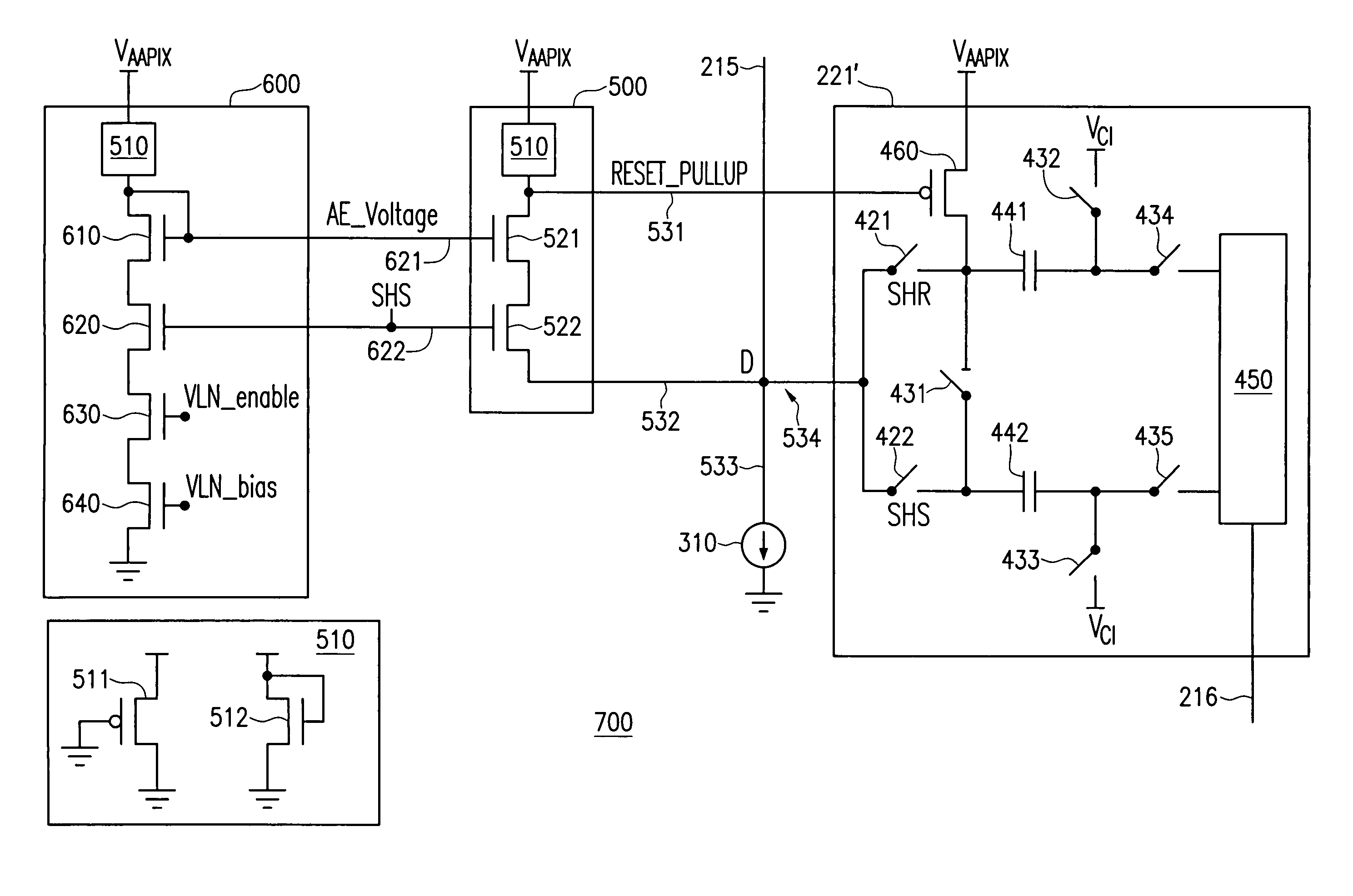
[0029] Now referring to the drawings, where like reference numerals designate like elements, there is shown in FIG. 6, column circuitry 220′ incorporating the anti-eclipse system of the present invention.

[0030] As illustrated, each column line 215 is associated with a processing block 700. Each column line 215 is used to provide to its associated processing block 700 a reset signal Vrst and a pixel signal Vsig (at different times). The processing block 700, as described in greater detail below, produces an analog pixel signal Vpixel, which is protected from eclipse distortion on line 216.

[0031]FIG. 7 is a more detailed illustration of processing block 700 of FIG. 6. The column line 215 is respectively coupled in parallel at node D via lines 532, 533, and 534 to a photo signal monitor circuit 500, a load circuit 310, and an analog processing circuit 221′. The photo signal monitor circuit 500 is also directly coupled to the analog processing circuit 221′ via line 531. Additionally, ...


PUM


Abstract

An anti-eclipse circuit for an imaging sensor monitors the photo signal level output by a pixel to determine whether the photo signal corresponds to the pixel being operated at a saturated state. If so, there is a risk that the pixel may be susceptible to an eclipse distortion. When the pixel is detected as being operated in a saturated state, the anti-eclipse circuit pulls up the reset signal level previously stored in a sample and hold circuit to an appropriate voltage level in order to prevent an eclipse distortion from arising.

Description

FIELD OF INVENTION [0001] The present invention relates generally to pixel architectures for semiconductor imagers. More specifically, the present invention relates to an anti-eclipse system for image sensors. BACKGROUND OF THE INVENTION [0002]FIG. 1 is an illustration of a conventional four transistor (4T) pixel 100. The pixel 100 includes a light sensitive element 101, shown as a photodiode, a floating diffusion node C, and four transistors: a transfer transistor 111, a reset transistor 112, a source follower transistor 113, and a row select transistor 114. The pixel 100 accepts a TX control signal for controlling the conductivity of the transfer transistor 111, a RST control signal for controlling the conductivity of the reset transistor 112, and a ROW select signal for controlling the conductivity of the row select transistor 114. The voltage at the floating diffusion node C controls the conductivity of the source follower transistor 113. The output of the source follow transist...

Claims


Application Information

Patent Timeline
IPC IPC(8): H04N5/335H04N5/357H04N5/376
CPCH04N5/3598H04N25/627H01L27/146H04N25/60H04N25/75
Inventor RYSINSKI, JEFFREYVINAYAGAMOORTHY, SANJAYAN
Owner MICRON TECH INC
Why Eureka
Try Eureka