High fill factor multi-way shared pixel

a multi-way shared, high-filling technology, applied in the field of digital image sensors, can solve the problems of undesirable phenomena, less efficient pixel cells, limited charge storage capacity, etc., and achieve the effect of increasing the potential fill factor, quantum efficiency and increasing the charge capacity of the pixel cell array

Active Publication Date: 2006-11-16
APTINA IMAGING CORP
View PDF19 Cites 128 Cited by
  • Summary
  • Abstract
  • Description
  • Claims
  • Application Information

AI Technical Summary

Benefits of technology

[0008] The present invention, in the various exemplary embodiments, provides a pixel cell array architecture having multiple pixel cells with shared pixel cell components. The pixel cell architecture increases the potential fill factor, and in turn, the quantum efficiency of the pixel cell array. The common pixel cell components may be shared by a number of pixels in the array, and may include several components that are associated with the readout of a signal from the pixel cells.
[0009] In accordance with exemplary embodiments of the invention, the pixel cell architecture includes a transfer gate which is angled with respect to the pixel cell's photosensor. In yet other exemplary embodiments, a storage capacitor is suitably located such that it can be shared by multiple pixel cells to increase the charge capacity of the pixel cells, while maintaining a high fill factor.

Problems solved by technology

In addition, conventional storage nodes, such as floating diffusion region 110, have a limited amount of charge storage capacity.
Once this capacity is reached, a pixel cell becomes less efficient.
Once the charge storage capacity is exceeded, an undesirable phenomenon occurs, whereby the “over-capacity” charges escape to undesirable parts of the pixel cell 100 or to adjacent pixel cells.
The problem with this solution, however, is that a capacitor on a pixel cell takes up space that could otherwise be used to increase the size of the photosensor, thereby decreasing the potential fill factor for the pixel cells and overall array.

Method used


Image

  • High fill factor multi-way shared pixel
  • High fill factor multi-way shared pixel
  • High fill factor multi-way shared pixel

Examples


Embodiment Construction

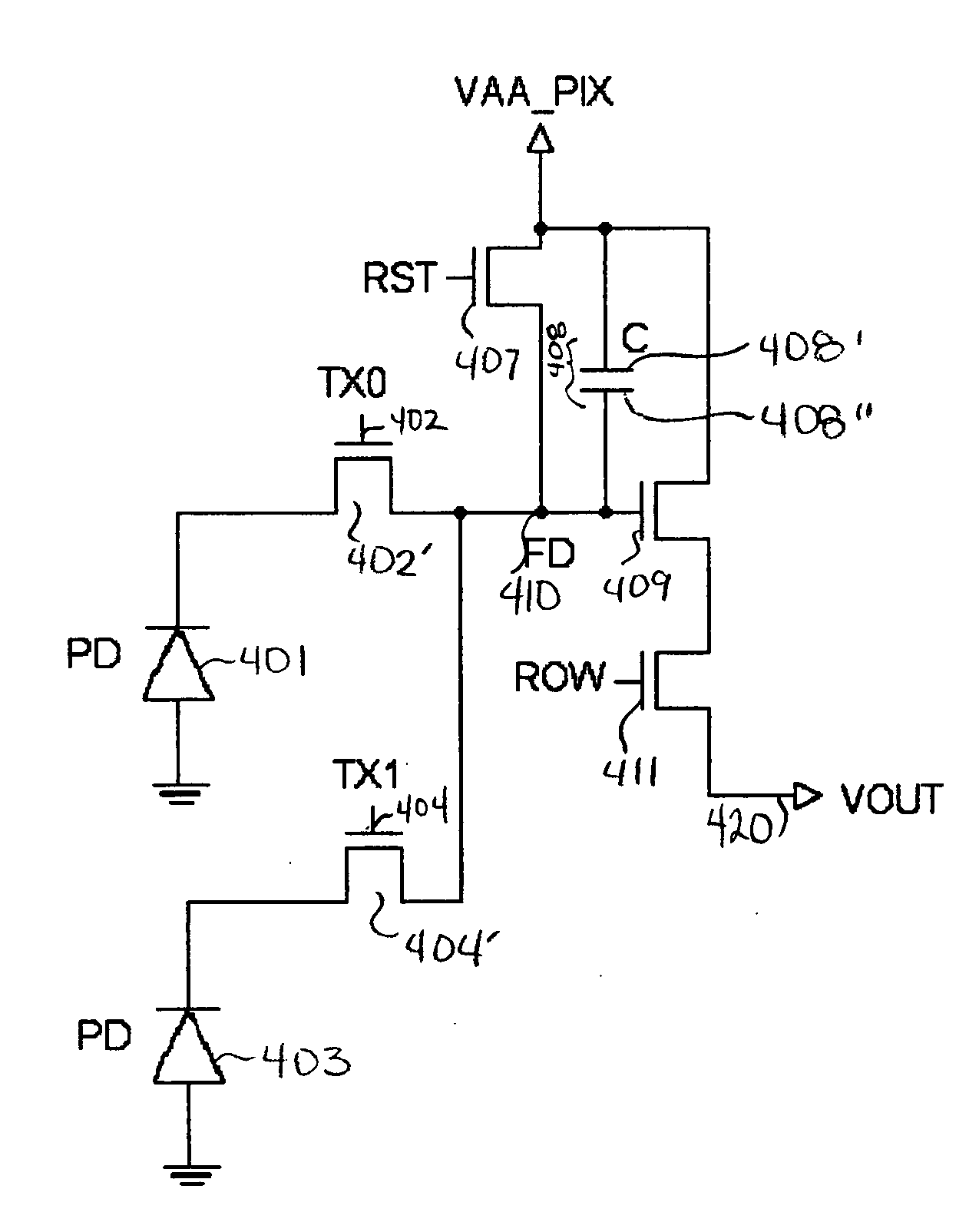
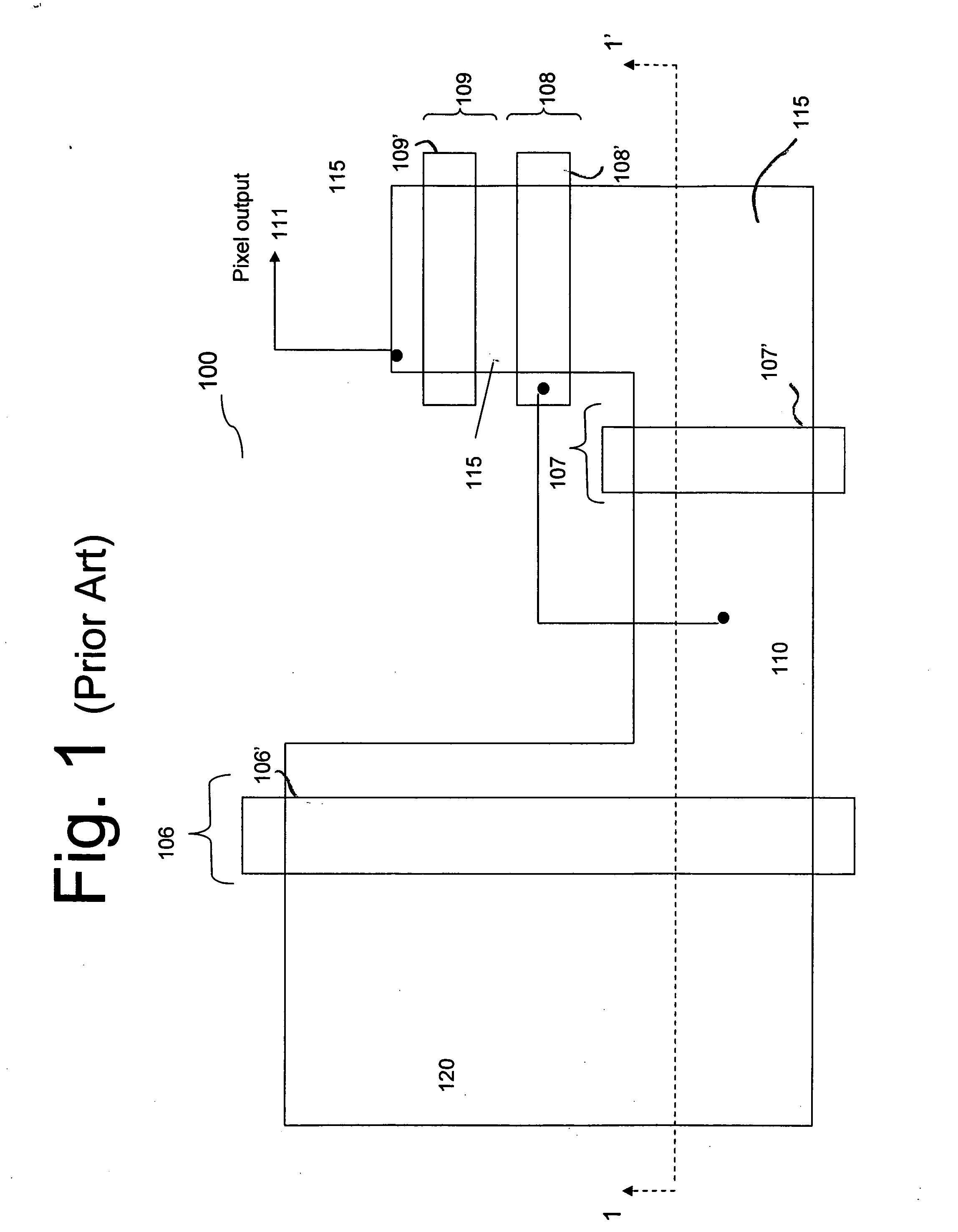
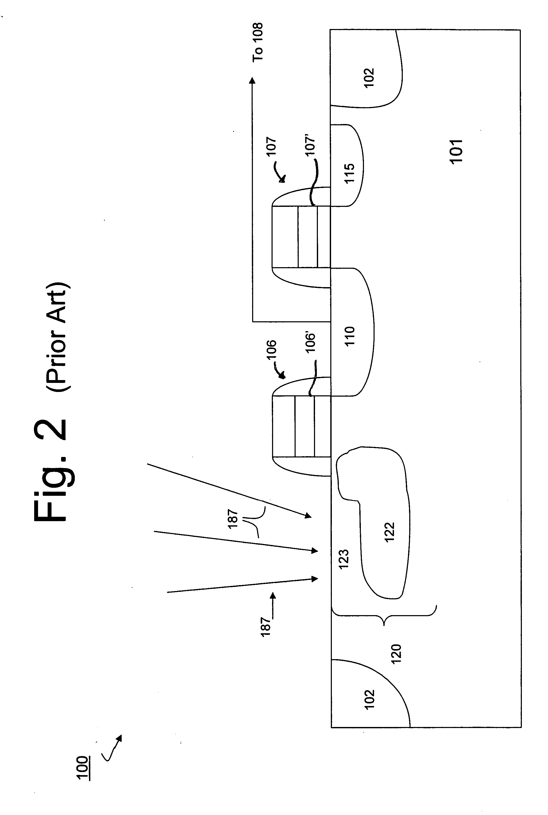
[0022] In the following detailed description, reference is made to the accompanying drawings, which form a part hereof and show by way of illustration specific embodiments in which the invention may be practiced. These embodiments are described in sufficient detail to enable those skilled in the art to practice the invention, and it is to be understood that other embodiments may be utilized, and that structural, logical, and electrical changes may be made without departing from the spirit and scope of the present invention. The progression of processing steps described is exemplary of embodiments of the invention; however, the sequence of steps is not limited to that set forth herein and may be changed as is known in the art, with the exception of steps necessarily occurring in a certain order.

[0023] The terms “wafer” and “substrate,” as used herein, are to be understood as including silicon, epitaxial, silicon-on-insulator (SOI) or silicon-on-sapphire (SOS) technology, doped and u...


PUM


Abstract

A pixel cell array architecture having a multiple pixel cells with shared pixel cell components. The individual pixel cell architecture increases the fill factor and the quantum efficiency for the pixel cell. The common pixel cell components may be shared by a number of pixels in the array, and may include several components that are associated with the readout of a signal from the pixel cell. Other examples of the pixel array architecture having improved fill factor for pixels in the array include an angled transfer gate and an efficiently located, shared capacitor.

Description

FIELD OF THE INVENTION [0001] The present invention relates generally to digital image sensors and in particular to a pixel cell array architecture having shared components among pixel cells of the array. BACKGROUND OF THE INVENTION [0002] Typically, a digital imager array includes a focal plane array of pixel cells, each one of the cells including a photosensor, e.g. a photogate, photoconductor, or a photodiode. In a CMOS imager a readout circuit is connected to each pixel cell which typically includes a source follower output transistor. The photosensor converts photons to electrons which are typically transferred to a floating diffusion region connected to the gate of the source follower output transistor. A charge transfer device (e.g., transistor) can be included for transferring charge from the photosensor to the floating diffusion region. In addition, such imager cells typically have a transistor for resetting the floating diffusion region to a predetermined charge level prio...

Claims


Application Information

Patent Timeline
Patent Type & Authority Applications(United States)
IPC IPC(8): H04N5/335
CPCH01L27/14603H01L27/14641H04N5/37452H04N3/155H04N25/59H04N25/778H04N25/771H01L27/146H04N25/77
Inventor MCKEE, JEFFREY A.SHAH, JOEY
Owner APTINA IMAGING CORP
Why Eureka
Try Eureka