
Formation of deep trench airgaps and related applications

a technology of air gap and deep trench, applied in the field of trench formation, can solve the problems of not being very scalable, many methods had certain process limitations, and the collector substrate capacitance is a significant contributor to the total switching delay, so as to reduce the width of the deep trench, reduce the total device area, and reduce the parasitic collector substrate perimeter capacitance.

Active Publication Date: 2006-11-16
INTERUNIVERSITAIR MICRO ELECTRONICS CENT (IMEC VZW)
View PDF17 Cites 19 Cited by
  • Summary
  • Abstract
  • Description
  • Claims
  • Application Information

AI Technical Summary

Benefits of technology

This approach effectively reduces the parasitic collector-substrate perimeter capacitance, optimizing device performance by minimizing switching delay and power consumption while maintaining low substrate noise and high breakdown voltage, and is scalable for advanced device designs.

Problems solved by technology

In Front End Of Line (FEOL) processing, isolation of the active device areas is one of the critical issues when dimensions are reduced.
Many of the methods had certain process limitations and were not very scalable.
In common-emitter stages designed in a low-power bipolar technology, the collector-substrate capacitance is a significant contributor to the total switching delay.
This fact imposes constraints on the selection of the process steps and on the location of the module in the complete process flow.
Although a complete oxide filling is preferred, because of its good isolation properties and low dielectric constant, this scheme is not easy to implement for several reasons.
Namely, it is difficult to obtain a complete fill of the deep trench without leaving any voids, and also because a completely oxide-filled deep trench would generate localized stresses and defects during and after processing.

Method used


Image

  • Formation of deep trench airgaps and related applications
  • Formation of deep trench airgaps and related applications
  • Formation of deep trench airgaps and related applications

Examples


Embodiment Construction

[0039] The following description and examples illustrate a preferred embodiment of the present invention in detail. Those of skill in the art will recognize that there are numerous variations and modifications of this invention that are encompassed by its scope. Accordingly, the description of a preferred embodiment should not be deemed to limit the scope of the present invention.

[0040] The term “sacrificial,” as used herein, is a broad term and is used in its ordinary sense, including, without limitation, a material or a layer that is deposited temporarily, and that is not supposed to remain, at least totally, in the final device, or a material or layer that is destined to be removed, at least partially, during the process of fabricating a device.

[0041] The term “spacer,” as used herein, is a broad term and is used in its ordinary sense, including, without limitation, a material or layer that is deposited on a side wall of a trench, hole, via, or other structure that is partially...


PUM


Abstract

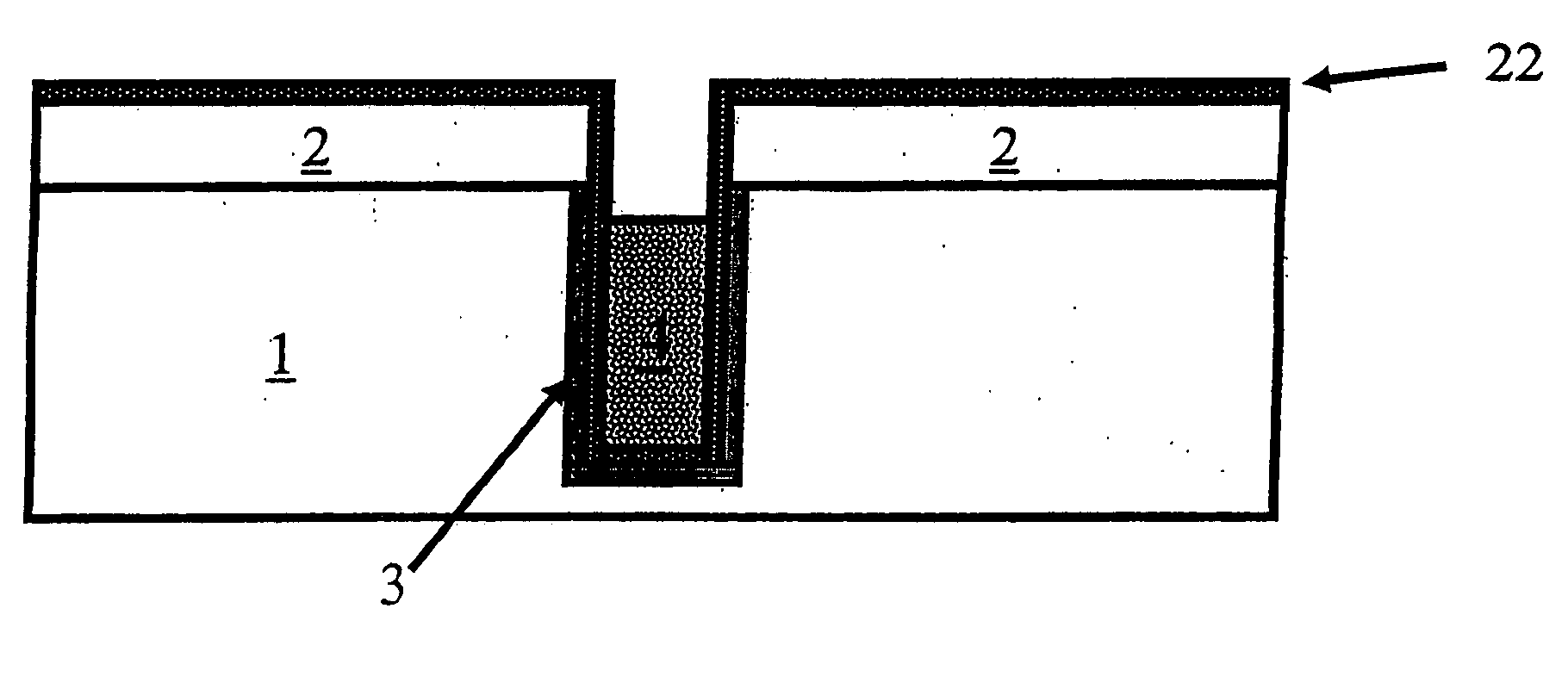
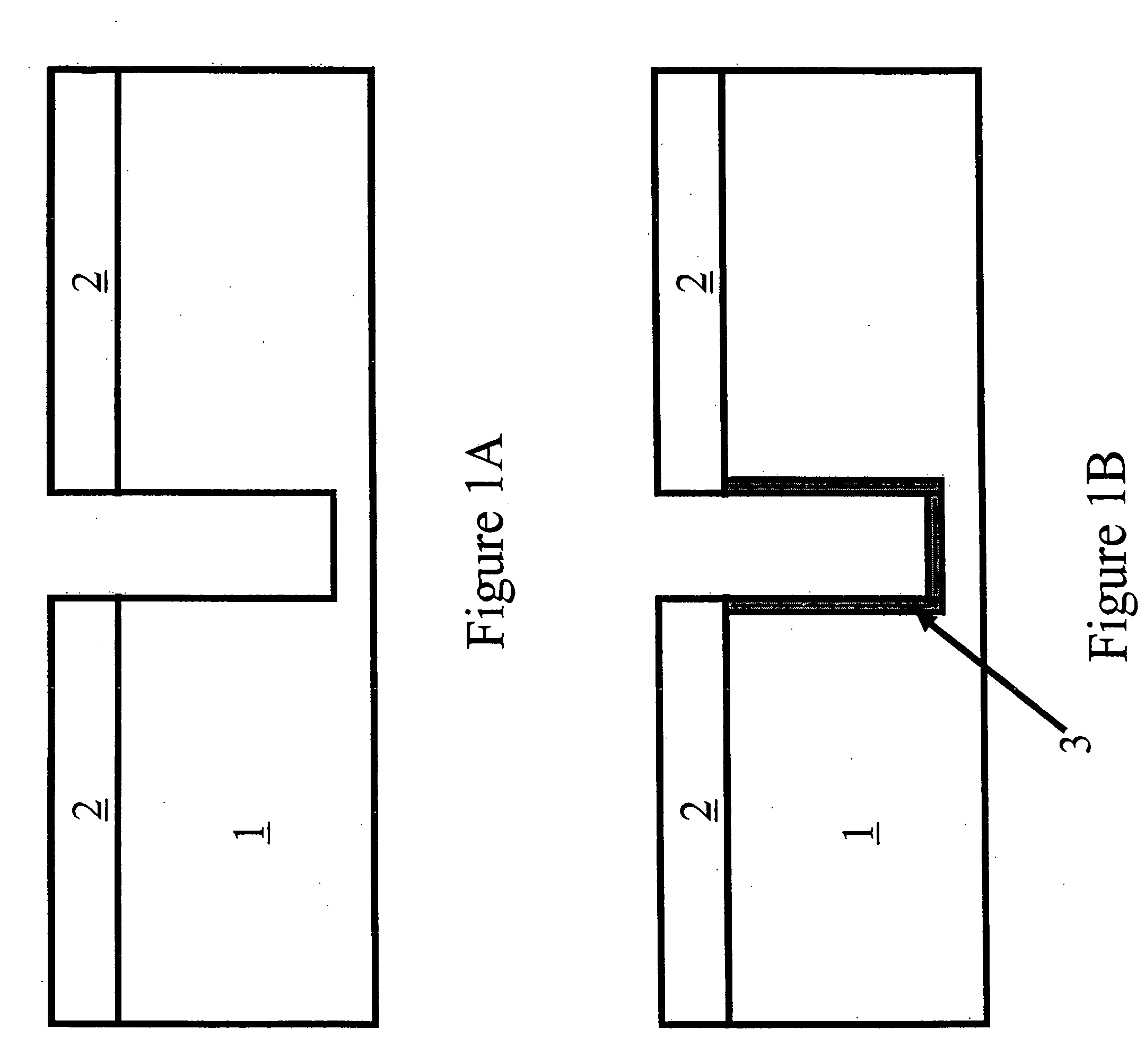
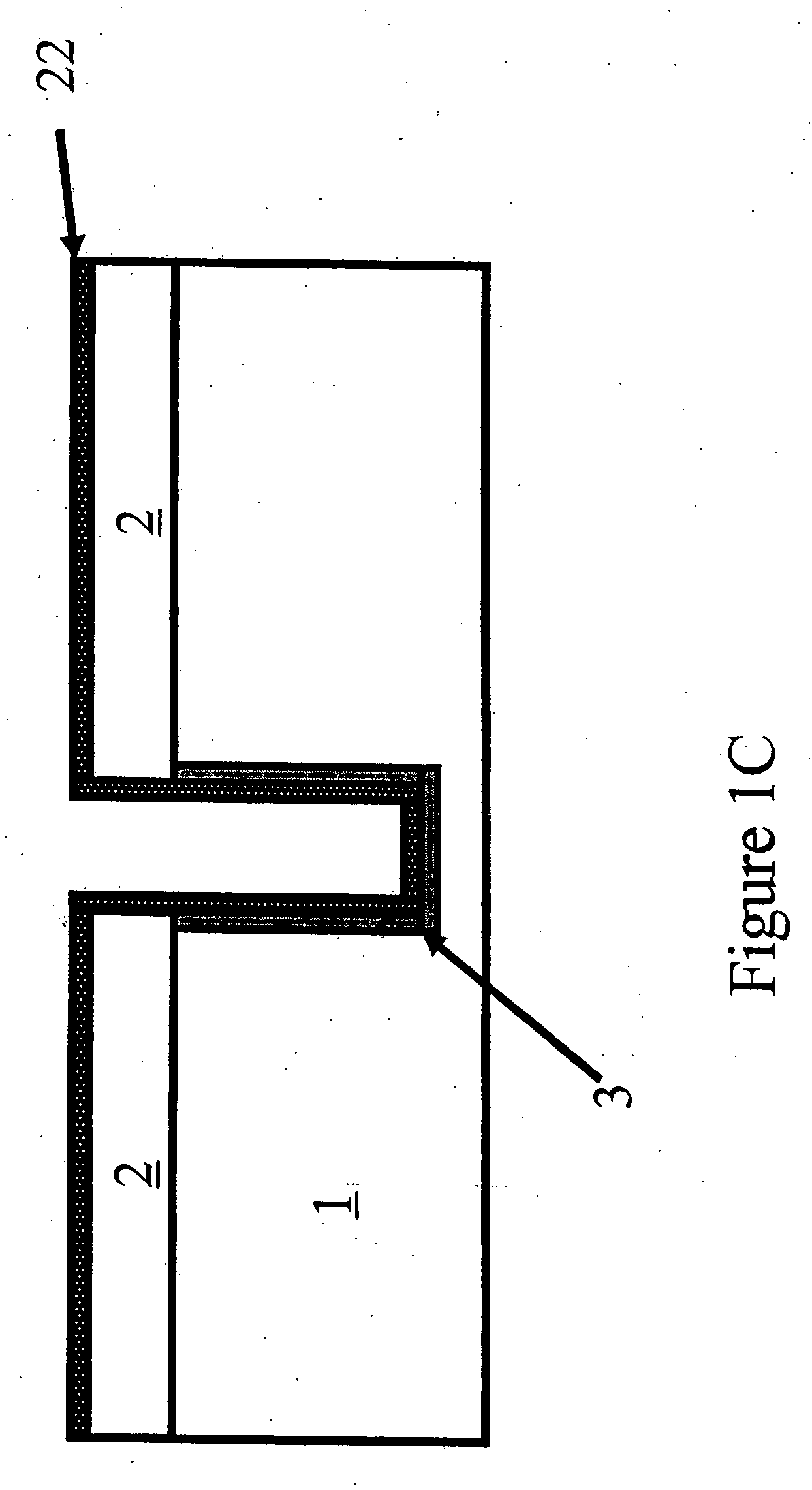
A method for forming deep trench or via airgaps in a semiconductor substrate is disclosed comprising the steps of patterning a hole in the substrate, partly fill said hole with a sacrificial material (e.g. poly-Si), depositing spacers on the sidewalls of the unfilled part of the hole (e.g. TEOS) to narrow the opening, removing through said narrowed opening the remaining part of the sacrificial material (e.g. by isotropic etching) and finally sealing the opening of the airgap by depositing a conformal layer (TEOS) above the spacers. The method of forming an airgap is demonstrated successfully for use as deep trench isolation structures in BiCMOS devices.

Description

RELATED APPLICATION [0001] This application is a division of U.S. application Ser. No. 11 / 048,642, filed Jan. 31, 2005, which claims the benefit of U.S. Provisional Application No. 60 / 637,288, filed Dec. 17, 2004, which is incorporated by reference herein in its entirety.FIELD OF THE INVENTION [0002] The present invention is related to the field of forming trenches or vias filled with a gas (air), also referred to as airgaps, in a semiconductor device. BACKGROUND OF THE INVENTION [0003] The semiconductor industry is continuously reducing the dimensions of devices. In Back End Of Line (BEOL) processing, there is an interest in reducing dimensions of conductive layers as well as in the separation of the different conductive structures from each other. Isolation of these structures therefore becomes extremely important, and low-k materials are used to replace conventional dielectric insulating materials. The trend is to move on to the incorporation of air, namely, so-called “air region...

Claims


Application Information

Patent Timeline
Patent Type & Authority Applications(United States)
IPC IPC(8): H01L21/8238H01L29/80
CPCH01L21/762H01L21/76289H01L21/764H01L21/76898H01L23/481H01L25/0657H01L25/50H01L2924/0002H01L2221/1094H01L2225/06513H01L2225/06541H01L2924/00
Inventor KUNNEN, EDDY
Owner INTERUNIVERSITAIR MICRO ELECTRONICS CENT (IMEC VZW)
Learn More