Scintillator panel and method of manufacturing radiation image sensor

a technology of radiation image sensor and scintillator, which is applied in the direction of radiation intensity measurement, instruments, x/gamma/cosmic radiation measurement, etc., can solve the problems of radiation image not being reduced in size using an optical system, scintillator cannot be uniformly vaporized, etc., and achieve the effect of preventing deliquescen

Inactive Publication Date: 2006-11-23
HAMAMATSU PHOTONICS KK
View PDF8 Cites 25 Cited by
  • Summary
  • Abstract
  • Description
  • Claims
  • Application Information

AI Technical Summary

Benefits of technology

[0009] Therefore, it is an object of the present invention to provide a manufacturing method of a scintillator panel and a radiation image sensor, with which the slimming down of the substrate and enlarging the area proportion of the scintillator forming surface on the substrate are facilitated.
[0011] With the manufacturing method for the scintillator panel according to the present invention, an auxiliary substrate is overlapped onto a substrate in forming a scintillator on the substrate. Since the auxiliary substrate is overlapped onto the substrate, warping of the substrate due to its own weight or the weight of the scintillator can be prevented in forming the scintillator. The warping of the substrate is likewise prevented even when the substrate has a large area. The scintillator can thus be formed uniformly on the substrate even when the substrate is thin or large in area.
[0013] By thus forming a scintillator on an organic film disposed on an auxiliary substrate and thereafter separating the organic film, on which the scintillator is formed, from the auxiliary substrate, a scintillator panel having the organic film itself as the substrate can be formed. By making thin the organic film provided here, a state wherein the scintillator is formed on a thin substrate can be realized. The same effects as those of the above-described case of manufacturing a scintillator panel by adding an auxiliary substrate to a substrate can be obtained in this case as well.
[0014] Preferably, a step of covering the organic film, having the scintillator and being separated from the auxiliary substrate, with a protective film is also included. The scintillator can thereby be prevented from contacting external air and undergoing deliquescence due to the moisture contained in the air and other physical and chemical degradation, damage, etc.
[0018] A step of forming a metal reflecting film between the substrate and the scintillator may be provided. The luminance of the light emitted from the scintillator can thereby be increased.
[0026] By thus mounting the scintillator, formed on the substrate or the film, onto the solid-state image pickup element, a radiation image sensor, with which the scintillator is formed uniformly on the substrate that is thin or large in area, can be manufactured. For the mounting of the scintillator or the substrate on the light receiving surface of the solid-state image pickup element, besides the embodiment directly mounting the scintillator or the substrate, an embodiment mounting via an organic film or a protective film is also possible. In order to prevent deliquescence, etc., of the scintillator, the scintillator is preferably covered with a protective film, and in this case, the exposed portions of the scintillator are covered. In regard to covering the exposed portions of the scintillator, besides the embodiment covering just the scintillator with the protective film, an embodiment covering at least one among the scintillator forming portion, the substrate, and the solid-state image pickup element along with the scintillator is also possible.

Problems solved by technology

However, in an attempt to manufacture a scintillator panel with a thin substrate by the above-described conventional method, the substrate becomes warped by its own weight when end portions of the substrate are placed on the holding jig and there will be a problem that scintillator cannot be vapor deposited uniformly.
This problem tends to occur especially when a substrate of large area is used.
Unlike a visible light image, a radiation image cannot be reduced in size using an optical system, and the above problem tends to occur readily since a scintillator panel of a large area in the excess of 30 centimeters square is required, for example, in chest X-ray image taking.

Method used


Image

  • Scintillator panel and method of manufacturing radiation image sensor
  • Scintillator panel and method of manufacturing radiation image sensor
  • Scintillator panel and method of manufacturing radiation image sensor

Examples


first embodiment

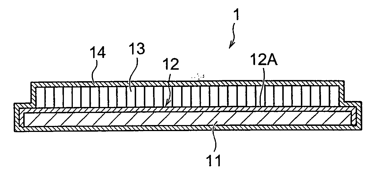
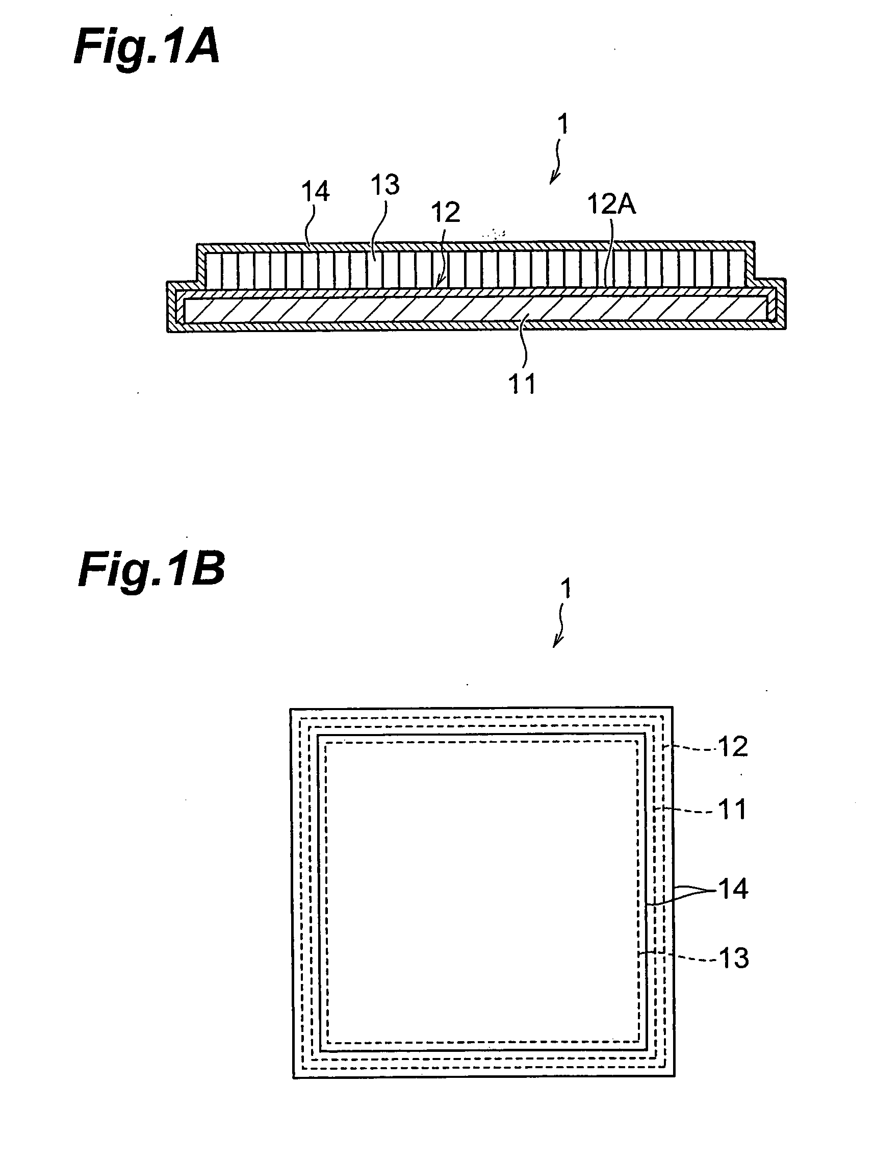
[0049]FIG. 1A is a sectional view of a scintillator panel manufactured by a manufacturing method of a first embodiment, and FIG. 1B is a plan view thereof. As shown in FIG. 1A and FIG. 1B, scintillator panel 1 of this embodiment has a radiation-transmitting substrate 11, composed of glass or amorphous carbon or other material having carbon as the main component. On one surface of substrate 11 (the upper surface in FIG. 1A) is formed an organic film 12, which covers the one surface of substrate 11. Organic film 12 covers the entire one surface of substrate 11 and is formed continuously across the side surfaces of substrate 11. Substrate 11 is a thin substrate and although it has a rectangular shape in plan view, it may instead have a circular shape, etc., in plan view. Organic film 12 is composed of a xylene-based resin, such as polyparaxylylene (parylene (trade name), made by Three Bond Co., Ltd.), polyparachloroxylylene (parylene C (trade name), made by Three Bond Co., Ltd.).

[0050]...

third embodiment

[0061] Next, the present invention shall now be described. FIG. 9A is a sectional view of a scintillator panel manufactured by a manufacturing method according to this embodiment, and FIG. 9B is a sectional view of a modification example thereof. As shown in FIG. 9A, with the scintillator panel 3 according to the present embodiment, scintillator 13 is formed on one surface of organic film 12, composed of polyparaxylylene, polyparachloroxylylene, or other xylene-based material, and organic film 12 and scintillator 13 are covered entirely by protective film 14. That is, with the present embodiment, organic film 12 serves in common as substrate 11.

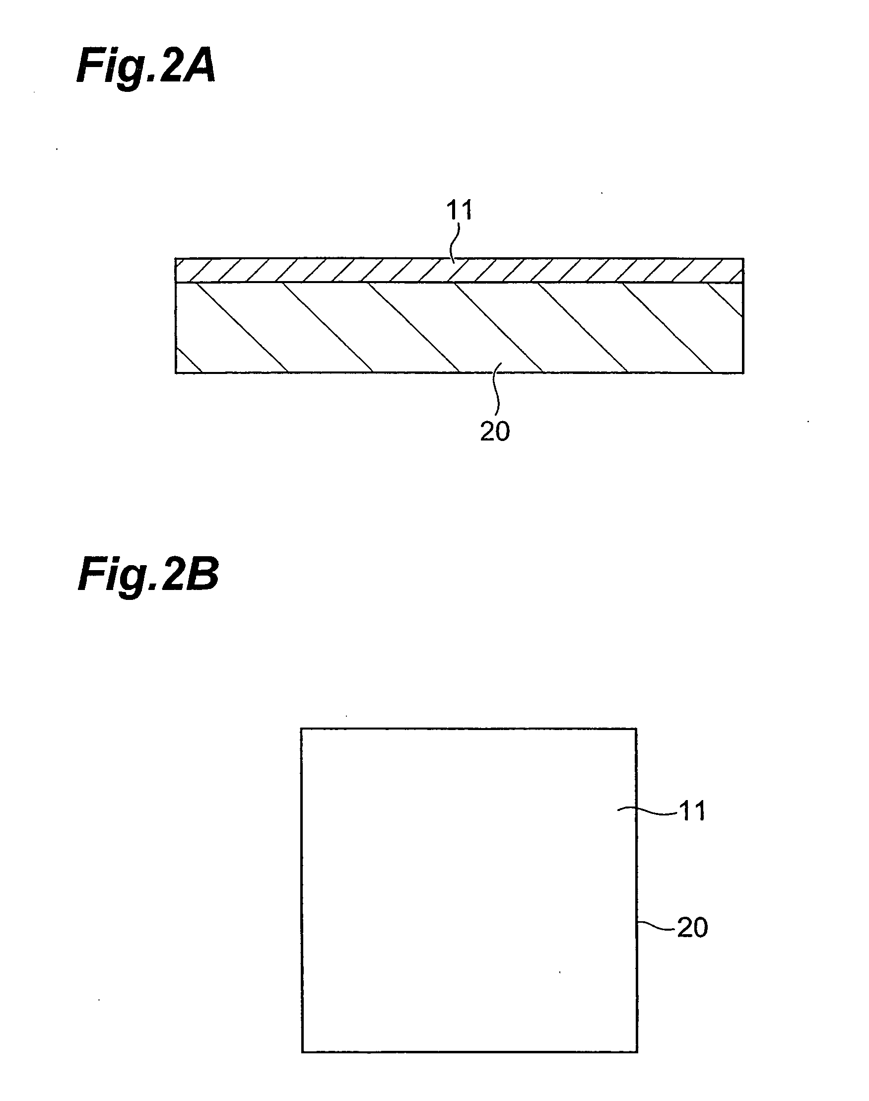
[0062] To describe the method of manufacturing this scintillator panel, first as shown in FIG. 10A and FIG. 10B, auxiliary substrate 20 for scintillator forming is prepared and the entirety of this auxiliary substrate is covered by organic film 12. This auxiliary substrate 20 has certain thickness and obviously it is preferably thicker than o...

fifth embodiment

[0070] this invention shall now be described. FIG. 14A is a sectional view of a scintillator panel manufactured by a manufacturing method according to the present embodiment, and FIG. 14B is a front view thereof. As shown in FIG. 14A and FIG. 14B, although scintillator 13 is set on substrate 11 in this scintillator panel 33, this scintillator 13 is formed on scintillator forming portion 12A, and an arrangement, wherein scintillator 13 is sandwiched by scintillator forming portion 12A and substrate 11, is employed. This substrate 11, scintillator 13, and scintillator forming portion 12A are covered by protective film 14. The present embodiment is of a mode wherein scintillator forming portion 12A is not used as it is as the substrate and another substrate is provided separately.

[0071] To describe the method of manufacturing scintillator panel 33 of the present embodiment, first, auxiliary substrate 20 is covered entirely with organic film 12 in the same manner as in the manufacturing...


PUM

PropertyMeasurementUnit
thicknessaaaaaaaaaa
radiation transmittanceaaaaaaaaaa
weightaaaaaaaaaa

Abstract

An auxiliary substrate 20 is overlapped onto a thin substrate 11, and substrate 11 and auxiliary substrate 20 are covered with an organic film 12. Thereafter, a scintillator 13 is formed on a scintillator forming portion 12A of organic film 12 that corresponds to substrate 11. Here, since thickness is added to substrate 11 by auxiliary substrate 20, the warping of substrate 11 is prevented and scintillator 13 is formed uniformly.

Description

TECHNICAL FIELD [0001] This invention relates to a scintillator panel and a radiation image sensor for X-ray image taking for medical and industrial applications, etc., and a manufacturing method of the same. BACKGROUND ART [0002] Conventionally X-ray sensitive films have been used for medical or industrial X-ray image taking, but the use of radiation imaging systems using radiation image sensors is spreading due to the aspects of convenience and preservation of the image taking results. With such a radiation imaging system, a radiation image is acquired as two-dimensionally arrayed pixel data in the form of electrical signals by means of a radiation image sensor, and the signals are processed by a processing device and displayed on a monitor. A scintillator panel, in which a scintillator is formed by vapor depositing scintillator components onto a substrate of aluminum, glass, or fused silica, etc., is used in the radiation image sensor, and such a scintillator panel is disclosed, ...

Claims


Application Information

Patent Timeline
Patent Type & Authority Applications(United States)
IPC IPC(8): C23C16/00G01T1/20G01T1/24G01T1/29
CPCG01T1/2928Y10T156/1052G01T1/2018G01T1/2002G01T1/2006
Inventor SATO, HIROTOSUZUKI, TAKAHARUSUGANUMA, MASAHIRO
Owner HAMAMATSU PHOTONICS KK
Why Eureka
Try Eureka