Solid-state imaging device

a solid-state imaging and imaging device technology, applied in the field of solid-state imaging devices, can solve the problems of increasing the chip deficiency rate, reducing production efficiency, increasing the leak current, etc., and preventing the area of the image cell from increasing. , the effect of reducing the noise of fixed patterns

Inactive Publication Date: 2010-11-18
ORMON CORP
View PDF12 Cites 11 Cited by
  • Summary
  • Abstract
  • Description
  • Claims
  • Application Information

AI Technical Summary

Benefits of technology

[0013]The present invention provides a solid state imaging device that reduces fixed pattern noise while preventing increases in the area of an image cell.
[0015]In this invention, when the intensity of incident light is high, the photocurrent flowing through the light reception element undergoes logarithm conversion, and the potential at the sense node is read as the photoelectric conversion signal. The photoelectric conversion signal includes fixed pattern noise. The reset signal includes the threshold voltage of the load transistor and amplification transistor and the transconductance of the amplification transistor that cause fixed pattern noise. Accordingly, generation of the difference between the photoelectric conversion signal and the reset signal obtains an image signal that does not include fixed pattern noise. Further, by forming a pixel with a single light reception element and four transistors, the ratio of the area occupied by a photodiode in a single pixel, or the aperture ratio, may be increased. Further, since an increase in the area of each pixel is suppressed, enlargement of the chip size is prevented, the chip deficiency rate is kept low, and the productivity rate is prevented from decreasing.
[0017]In this invention, when the intensity of incident light is low, the photocurrent flowing through the light reception element undergoes linear conversion, and the potential at the sense node is read as the photoelectric conversion signal. The photoelectric conversion signal includes fixed pattern noise. The reset signal includes the threshold voltage of the load transistor and amplification transistor and the transconductance of the amplification transistor that cause fixed pattern noise. Accordingly, generation of the difference between the photoelectric conversion signal and the reset signal obtains an image signal that does not include fixed pattern noise. Further, by forming a pixel with a single light reception element and four transistors, the ratio of the area occupied by a photodiode in a single pixel, or the aperture ratio, may be increased. Further, since an increase in the area of each pixel is suppressed, enlargement of the chip size is prevented, the chip deficiency rate is kept low, and the productivity rate is prevented from decreasing.
[0019]In this invention, the photocurrent flowing through the light reception element is converted, and the potential at the sense node is read as a photoelectric conversion signal. The photoelectric conversion signal includes fixed pattern noise. The first reset signal includes the threshold voltage of the load transistor and amplification transistor and the transconductance of the amplification transistor that cause fixed pattern noise. The second reset signal includes the threshold voltage and transconductance of the amplification transistor. Accordingly, when the intensity of incident light is high in the light reception element, photocurrent undergoes logarithm conversion. Thus, the generation of the difference between the photoelectric conversion signal, which has undergone logarithm conversion, and the first reset signal obtains an image signal that does not include fixed pattern noise. When the intensity of intensity light is low in the light reception element, photocurrent undergoes linear conversion. In this case, the difference between the photoelectric conversion signal and the first reset signal does not include the threshold voltage of the first transistor. The difference between the first reset signal and the second reset signal is obtained to obtain the threshold voltage of the first transistor. Therefore, by adding the difference between the first reset signal and the second reset signal to the difference between the photoelectric conversion signal and the first reset signal, fixed pattern noise is eliminated from an image signal when the intensity of incident light is low. Further, by forming a pixel with a single light reception element and four transistors, the ratio of the area occupied by a photodiode in a single pixel, or the aperture ratio, may be increased. Further, since an increase in the area of each pixel is suppressed, enlargement of the chip size is prevented, the chip deficiency rate is kept low, and the productivity rate is prevented from decreasing.
[0022]As described above, the present invention reduces fixed pattern noise and prevents the area of the image cell from increasing.

Problems solved by technology

The FPN is a problem that must also be coped with in devices other than a logarithm conversion type imaging device.
This increases the chip deficiency rate and lowers production efficiency.
This increases the leak current, or dark current, caused by the added elements.

Method used


Image

  • Solid-state imaging device
  • Solid-state imaging device
  • Solid-state imaging device

Examples


first embodiment

[0030]A solid state imaging device 10 according to the present invention will now be discussed with reference to the drawings.

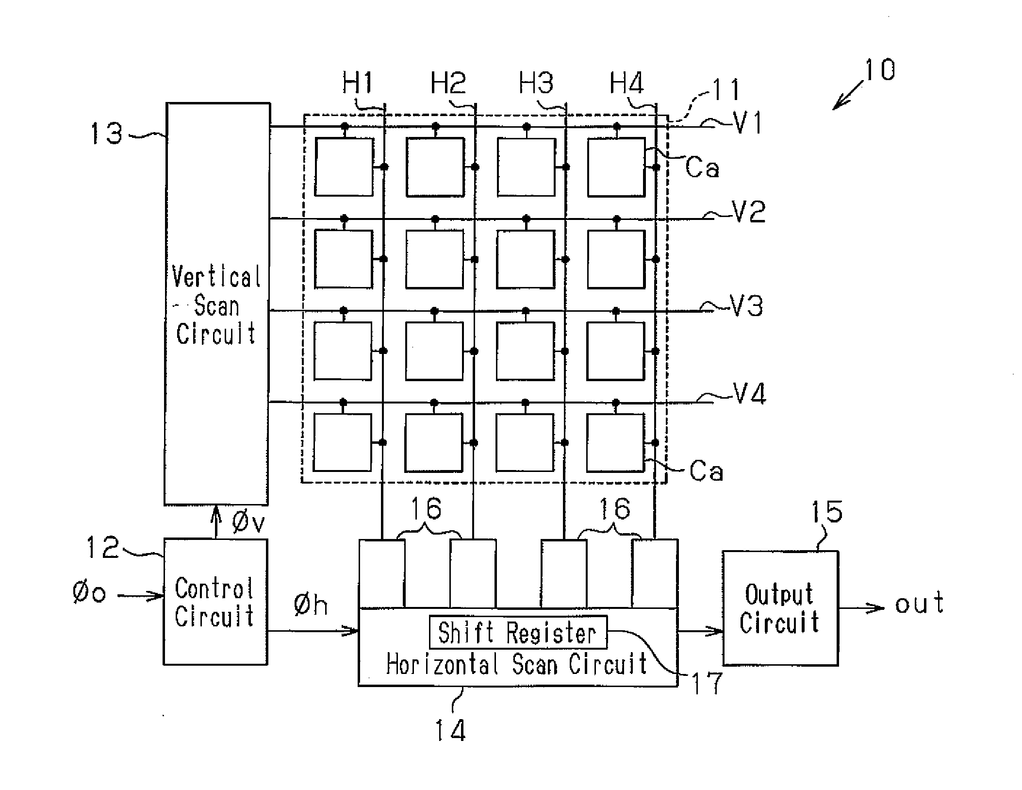
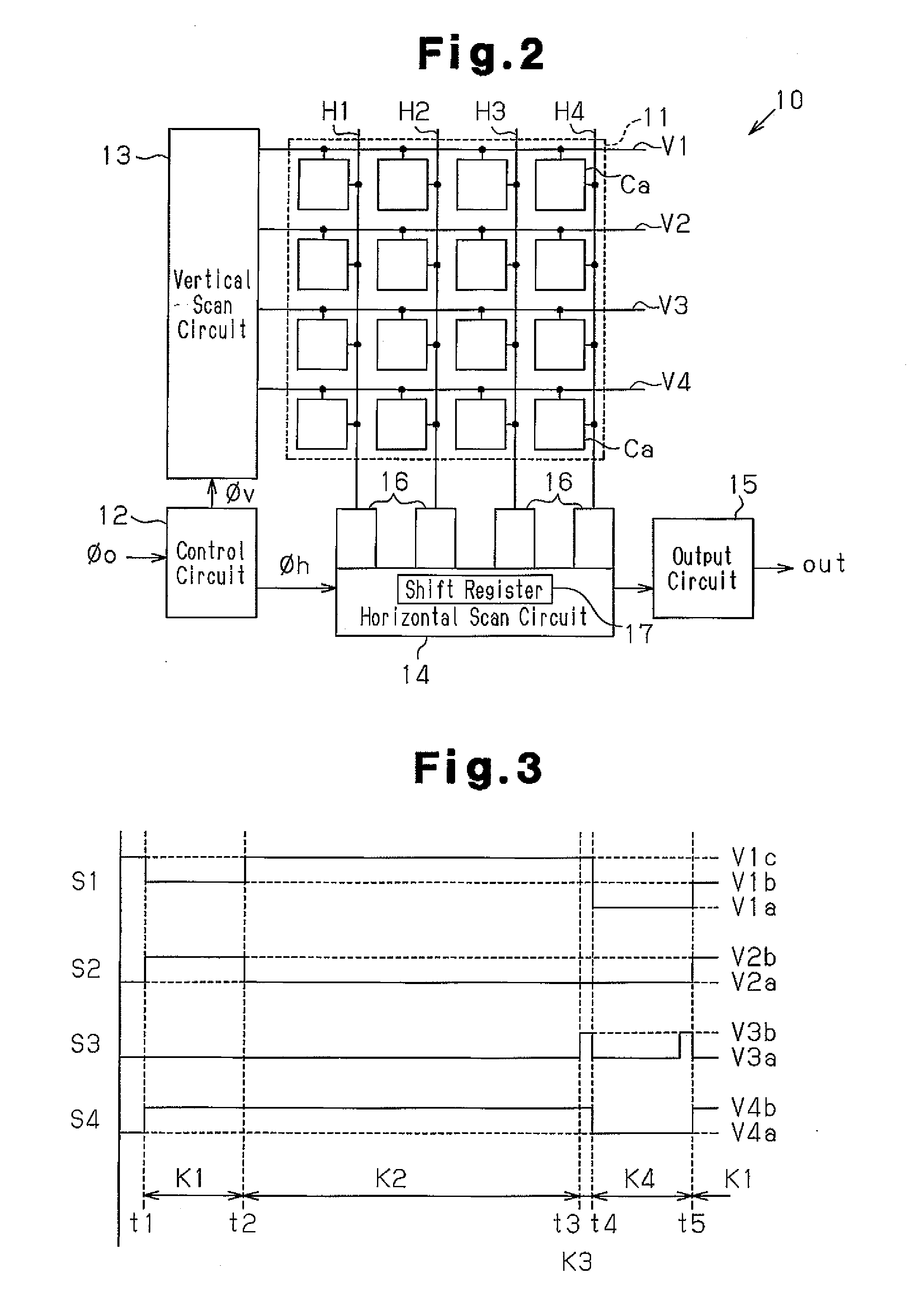
[0031]FIG. 2 is a schematic block circuit diagram of the solid state imaging device 10.

[0032]The solid state imaging device 10 includes an imaging unit 11, a control circuit 12, a vertical scan circuit 13, a horizontal scan circuit 14, and an output circuit 15.

[0033]The imaging unit 11 includes a plurality of pixels Ca arranged in a matrix. For the sake of brevity, the first embodiment will be discussed with the imaging unit 11 including 16 pixels Ca that are arranged in a matrix of four columns and four rows.

[0034]Based on a clock signal Φ0, the control circuit 12 generates a vertical clock signal Φv, which serves as a selection signal for selecting a row in the imaging unit 11, a horizontal clock signal Φh, which serves as a selection signal for selecting a column in the imaging unit 11, and a control signal for controlling and driving the pixels Ca and the...

second embodiment

[0067]the present invention will now be discussed with reference to the drawings.

[0068]The second embodiment differs from the first embodiment in drive waveform of a pixel so that the pixel ca is properly driven when generating a dark image.

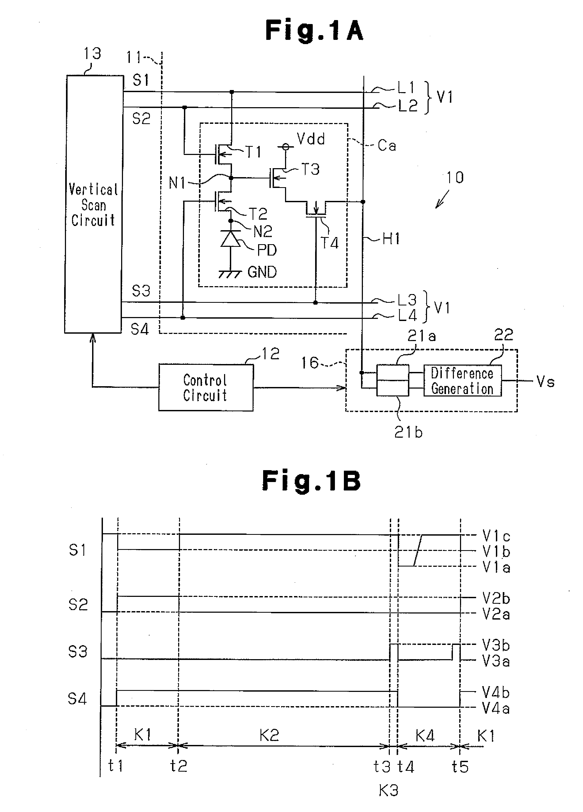
[0069]The vertical scan circuit 13 shown in FIG. 1A varies the drive signals as shown in FIG. 3 in response to a control signal from the control circuit 12.

[0070]During a photoelectric conversion period K2 from time t2 to time t3, the vertical scan circuit 13 provides the drive signals S1 to S4 to the signal lines L1 to L4 in the same manner as in the first embodiment. The potential at the sense node N1 when a dark image is generated, or when the intensity of the incident light is low, is determined as described below.

[0071]When a dark image is generated, or when the intensity of the incident light is low, the photocurrent Ip flowing through the photodiode PD is small. Thus, the potential at the sense node N1 does not shift to the normal state du...

third embodiment

[0085]the present invention will now be discussed with reference to the drawings.

[0086]In the third embodiment, components that are the same as those in the first and second embodiment are denoted with the same reference numerals.

[0087]Referring to FIG. 4, the CDS circuit 16 of the third embodiment includes three SH circuits 31a, 31b, and 31c, two difference generation circuits 32a and 32b, an adder circuit 33, a comparison circuit 34, and a selection circuit 35.

[0088]The SH circuits 31a to 31c, which are connected to the column signal line H1, hold a signal of the column signal line H1. The signal held by the first SH circuit 31a is provided to the first differential generation circuit 32a. The signal held by the second SH circuit 31b is provided to the first difference generation circuit 32a and second difference generation circuit 32b. The signal held by the third SH circuit 31c is provided to the second differential generation circuit 32b.

[0089]The first difference generation c...


PUM


Abstract

Suppressing increases in the area of an image cell while reducing fixed pattern noise (FPN). A photoelectric conversion signal is generated from photocurrent flowing through a photodiode (PD) in a pixel (Ca). A first transistor functioning as a load transistor is driven to operate in a strong inversion state and then operate in a subthreshold range. When the first transistor (T1) is operating in a subthreshold range, the potential at a sense node (N1) is read as a reset signal. Further, the difference between the photoelectric conversion signal and the reset signal is calculated to generate an image signal (Vs).

Description

FIELD OF THE INVENTION[0001]The present invention relates to a solid state imaging device.BACKGROUND OF THE INVENTION[0002]In the prior art, a MOS type imaging device is used to obtain various image data. Such an imaging device reads the charge accumulated in a pn junction capacitor of a photodiode through a MOS type transistor (e.g., field effect transistor (FET)).[0003]Generally, the latitude, or dynamic range, of a MOS type imaging device is said to be narrower than that of a photographic negative film. If the latitude is narrow, dark parts of an image are recorded as black pixel data, and bright parts of an image are recoded as white pixel data.[0004]A logarithm conversion type imaging device widens the dynamic range. As shown in FIG. 6, the imaging device includes an image cell formed by a photodiode PD, a load transistor T51, an amplification transistor T52, and a selection transistor T53. The cathode of the photodiode PD is connected to the source of the transistor T51, and t...

Claims


Application Information

Patent Timeline
Patent Type & Authority Applications(United States)
IPC IPC(8): H04N5/335H04N5/217H04N5/355H04N5/357H04N5/365H04N5/374
CPCH04N5/2176H04N5/35518H04N5/374H04N5/3651H04N5/3575H04N25/63H04N25/573H04N25/616H04N25/671H04N25/76
Inventor HASHIMOTO, MASASHI
Owner ORMON CORP
Why Eureka
Try Eureka