AI technical title is built by Patsnap AI team. It summarizes the technical point description of the patent document.
a microelectronic and integrated circuit technology, applied in the direction of electrical equipment, semiconductor devices, semiconductor/solid-state device details, etc., can solve the problems of increased intra-level interaction, increased energy consumption, and increased ic risk at line level, and achieve the effect of robust mechanical stability and the biggest impact on rc delay
Inactive Publication Date: 2006-11-23
GLOBALFOUNDRIES INC
View PDF30 Cites 1 Cited by
Summary
Abstract
Description
Claims
Application Information
AI Technical Summary
This helps you quickly interpret patents by identifying the three key elements:
Problems solved by technology
Method used
Benefits of technology
Benefits of technology
This approach results in a mechanically stable IC structure with the lowest possible effective dielectric constant at line levels, reducing RC delay and energy consumption while maintaining robustness, compatible with current microelectronicsprocessing standards.
Problems solved by technology
A major problem with increased density is the increased intralevel interaction in capacitive voltagecoupling and cross-talk between conductive lines, the largest component of which is between adjacent conductive lines in a given line level.
As a result of this increased interaction, the IC is at great risk for failure at line level, in the form of unacceptably slow signal propagation, i.e. Resistance-Capacitance (R-C) delay and increased energy consumption.
While these materials all have low K, the value is not as low as the ideal value of air and, as described in the Nag et al. patent, each may come with its own alternate limitations when left as the wiring level dielectric.
The presence of a liner on the wiring, however, risks raising the effective K. In U.S. Pat. No. 6,350,672 B1 to Sun there is no liner described.
Image
Click on the blue label to locate the original text in one second.
Reading with bidirectional positioning of images and text.
Examples
Embodiment Construction
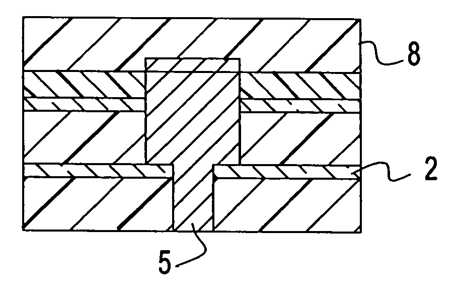
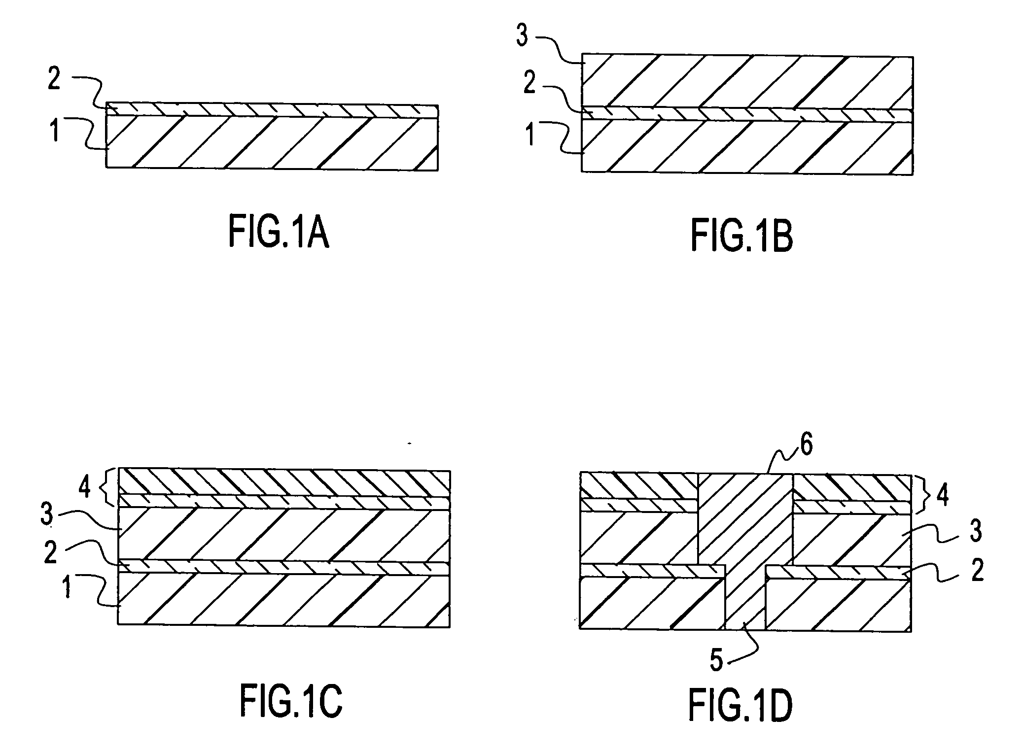
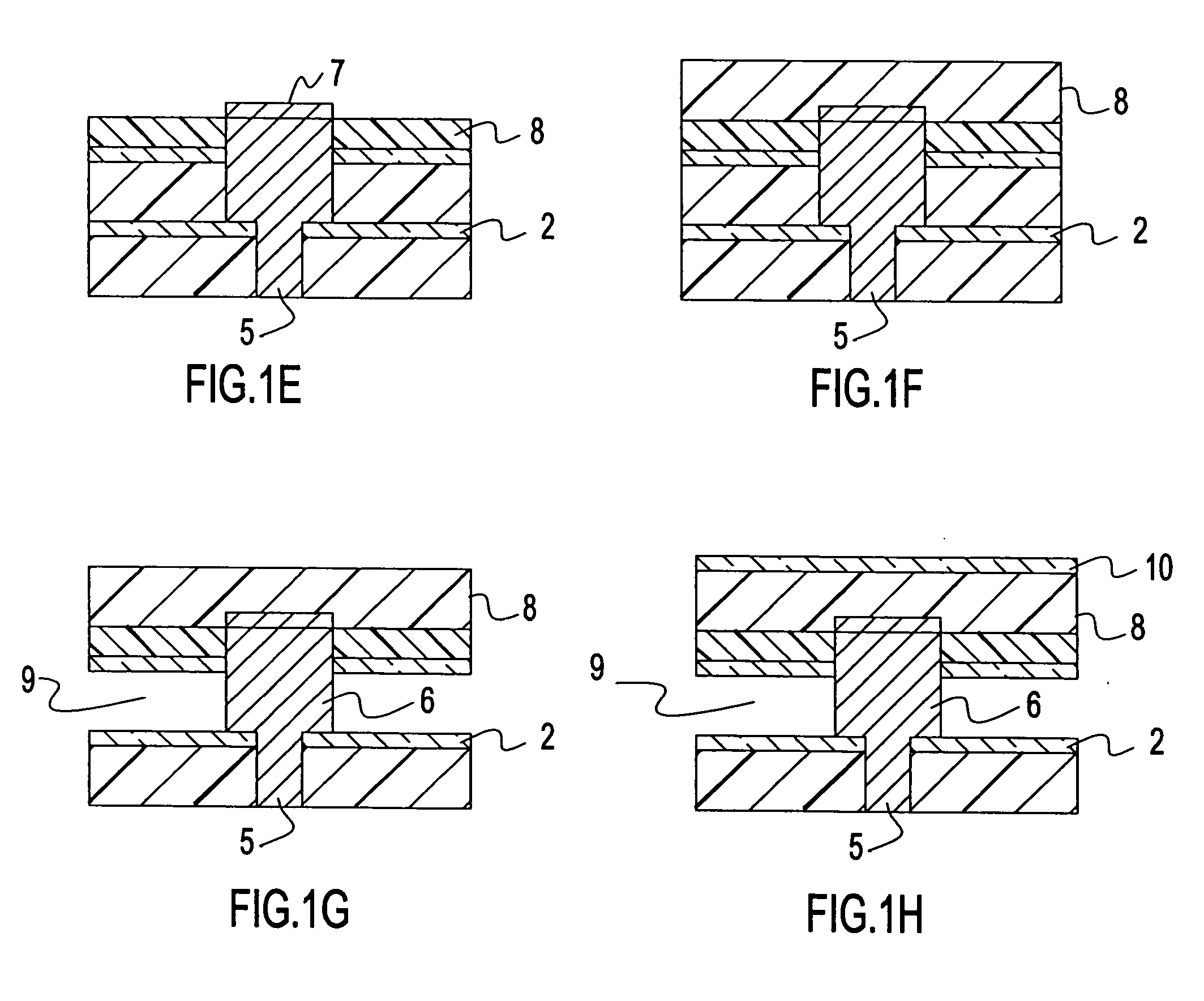
[0021]FIG. 1A shows the initial fabrication steps on the top surface of a semiconductor substrate (not shown) of an IC structure of the present invention. The first layer of a solid permanent ultra-low-K dielectric material 1 has been deposited on the substrate for patterning of the first via level. Examples of suitable porous and substantially non-porous gas permeable materials used to function as the solid permanent low-K dielectric at via levels include: porous SiLK and SiLK, a polymer product of Dow Chemical Company, which is applied as a spin-coated oligomeric solution and cured at about 400° C.-450° C.; porous SiCOH and SiCOH, a glassy spin-on material such as JSR, a product of JSR Micro; and methyl silsesquioxane (MSSQ). A first gas impermeable etch stop layer 2 has been deposited on the layer of permanent dielectric material 1 by means known in the art, such as spin-on, chemical vapor deposition (CVD) and the like. Examples of suitable materials used to function as the etch ...
PUM
Abstract
In a multilevel microelectronic integrated circuit, air comprises permanent line leveldielectric and ultra low-K materials are via level dielectric. The air is supplied to line level subsequent to removal of sacrificial material by clean thermal decomposition and assisted diffusion of byproducts through porosities in the IC structure. Optionally, air is also included within porosities in the via level dielectric. By incorporating air to the extent produced in the invention, intralevel and interlevel dielectric values are minimized.
Description
RELATED APPLICATIONS [0001] This application is a divisional of U.S. application Ser. No. 10 / 731,377, filed Dec. 8, 2003.BACKGROUND OF THE INVENTION [0002] The present invention relates to high density multilevel microelectronic integrated circuit (IC) structures. In particular, the present invention relates to the reduction of dielectric constant between conductive lines in each line level by providing air dielectric. A porous permanent dielectric in via levels is provided in order to optimize further the performance of the structure in a functioning device. [0003] An aggressive drive continues toward increasing the density of features in the IC structure and toward decreasing the size of individual features. At present, feature dimensions can be fabricated to be as small as about 0.5 microns or less, and may be separated by less than 5000 Angstroms. As the drive continues, materials and processes by which the IC structure is composed must be reexamined in order to deal with proble...
Claims
Application Information
Patent Timeline
Application Date:The date an application was filed.
Publication Date:The date a patent or application was officially published.
First Publication Date:The earliest publication date of a patent with the same application number.
Issue Date:Publication date of the patent grant document.
PCT Entry Date:The Entry date of PCT National Phase.
Estimated Expiry Date:The statutory expiry date of a patent right according to the Patent Law, and it is the longest term of protection that the patent right can achieve without the termination of the patent right due to other reasons(Term extension factor has been taken into account ).
Invalid Date:Actual expiry date is based on effective date or publication date of legal transaction data of invalid patent.
Patent Type & AuthorityApplications(United States)

