

Capacitor device, semiconductor devioce, and setting method of terminal capacitance of pad electrode thereof
a technology of capacitance value and capacitor, which is applied in the direction of semiconductor devices, semiconductor/solid-state device details, electrical apparatus, etc., can solve the problems of reducing the transmission speed of signals, difficult to fine-tune the capacitance value, and affecting the accuracy of semiconductor devices, etc., to achieve high accuracy
- Summary
- Abstract
- Description
- Claims
- Application Information
AI Technical Summary
Benefits of technology
Problems solved by technology
Method used
Image

Examples
first embodiment
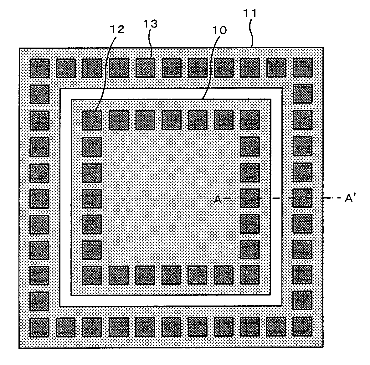
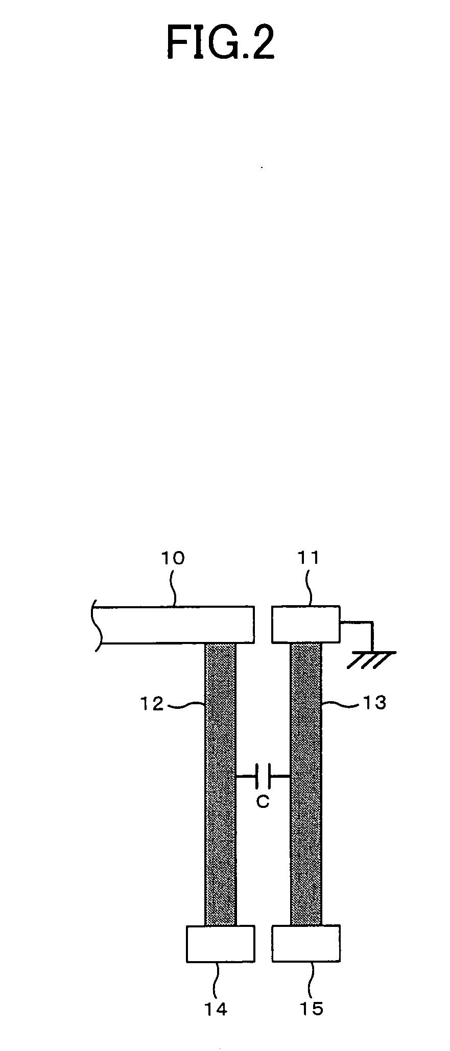
[0035] In the first embodiment, the present invention is applied to a semiconductor device in which a pad electrode is formed as an input / output terminal on a semiconductor substrate, based on the configuration of FIGS. 1 and 2. FIG. 1 shows a plan view of the pad electrode and its surroundings in the semiconductor device of the first embodiment, and FIG. 2 shows a cross-sectional view along the line A-A′ in the configuration of FIG. 1. In the semiconductor device of the first embodiment, a rectangular pad electrode 10 and a band-shaped surrounding wiring 11 which surrounds the entire pad electrode 10 are formed. The pad electrode 10 and the surrounding wiring 11 are formed, for example, on an upper aluminum wiring layer of the semiconductor device, and electrically insulated from each other by insulating films spaced a predetermined distance.
[0036] The pad electrode 10 is used as a connection terminal for inputting and outputting signals between the semiconductor device and the ou...
second embodiment
[0042] In the second embodiment, the present invention is applied to a semiconductor device in which a pad electrode is formed, based on the configuration of FIG. 3. FIG. 3 shows a plan view of the pad electrode and its surroundings in the semiconductor device of the second embodiment. In the semiconductor device of the second embodiment, a pad electrode 20 and a band-shaped surrounding wiring 21 which surrounds the pad electrode 20 are formed on a semiconductor substrate, and are the same in size and shape as in the first embodiment. Meanwhile, in the second embodiment, a via 22 formed in the pad electrode 20 and a via 23 formed in the surrounding wiring 21 are respectively different in structure from the vias 12 and 13 in the first embodiment.
[0043] As shown in FIG. 3, the via 22 of the pad electrode 20 and the via 23 of the surrounding wiring 21 are each formed in the shape of a single slit. That is, it is a feature of the second embodiment that each of vias 22 and 23 is a singl...
third embodiment
[0047] In the third embodiment, the present invention is applied to a semiconductor device in which a pad electrode is formed, based on the configuration of FIGS. 4 and 5. FIG. 4 shows a plan view of the pad electrode and its surroundings in the semiconductor device of the third embodiment, and FIG. 5 shows a cross-sectional view along the line B-B′ in the configuration of FIG. 4. In the semiconductor device of the third embodiment, in addition to a pad electrode 30 and a surrounding wiring 31, on the semiconductor substrate, a pad connecting portion 30a electrically connected to the pad electrode 30 is formed, which is a conductive region attached to one end of the pad electrode 30. The surrounding wiring 31 and the pad connecting portion 30a each have a number of lines and form a plurality of lines arranged alternately around the pad electrode 30. In this case, the pad electrode 30 and the pad connecting portion 30a are insulated from the surrounding wiring 31 by the insulating fi...
PUM
 Abstract
Description
Claims
Application Information