Semiconductor device and manufacturing method thereof

a technology of semiconductor devices and semiconductors, applied in semiconductor devices, semiconductor/solid-state device details, electrical apparatus, etc., can solve problems such as electrical failure and transmission loss, and achieve the effects of improving the propagation characteristics of signals received from or transmitted to antennas, excellent electromagnetic shielding properties, and high performan

Inactive Publication Date: 2006-11-30
SEMICON ENERGY LAB CO LTD
View PDF16 Cites 61 Cited by
  • Summary
  • Abstract
  • Description
  • Claims
  • Application Information

AI Technical Summary

Benefits of technology

[0019] According to the invention, a conductive layer is provided to surround a signal wiring layer; therefore, the propagation characteristics of a signal received from or transmitted to an antenna can be improved. Further, excellent electromagnetic shielding properties can prevent an integrated circuit from interfering with signal wires. Accordingly, a semiconductor device with high performance and high reliability can be provided.

Problems solved by technology

If signals are communicated between an integrated circuit and an antenna through a signal line, enough propagation characteristics cannot be obtained depending on the frequency, which results in transmission losses.
In addition, electromagnetic shielding properties of the signal line are not enough, leading to electrical failure such as interference with signal wires of the integrated circuit.

Method used


Image

  • Semiconductor device and manufacturing method thereof
  • Semiconductor device and manufacturing method thereof
  • Semiconductor device and manufacturing method thereof

Examples


embodiment mode 1

[0037] In this embodiment mode, an example of a semiconductor device of the invention is described with reference to FIGS. 1A and 1B.

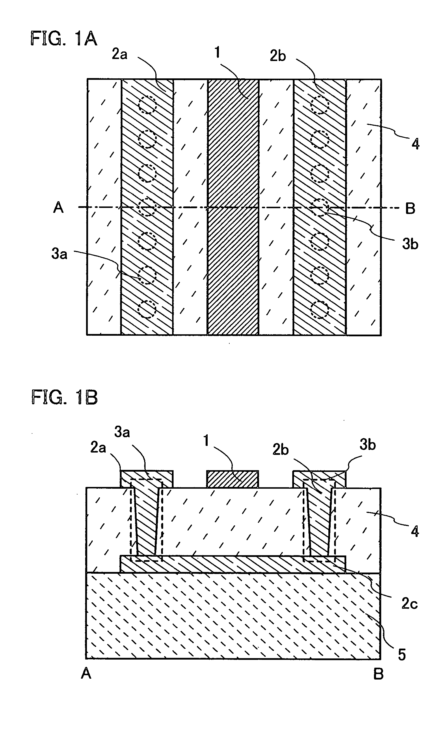
[0038]FIG. 1A is a top view of a semiconductor device of this embodiment mode, and FIG. 1B is a cross sectional view along a line A-B. The semiconductor device of this embodiment mode has a signal wiring layer 1 for a signal received from or transmitted to an antenna, a conductive layer 2a, a conductive layer 2b, a conductive layer 2c, an insulating layer 4 including an opening 3a and an opening 3b, and an insulating layer 5. The conductive layer 2a, the conductive layer 2b, and the conductive layer 2c are referenced to a signal (e.g., radio frequency signal) received from or transmitted to the signal wiring layer, and are set to an arbitrary potential. The conductive layer 2a and the conductive layer 2b are connected to the conductive layer 2c with a plurality of vias (the opening 3a and the opening 3b) along the propagation direction of a signal.

[0...

embodiment mode 2

[0042] In this embodiment mode, an example of a semiconductor device of the invention is described with reference to FIGS. 2A and 2B.

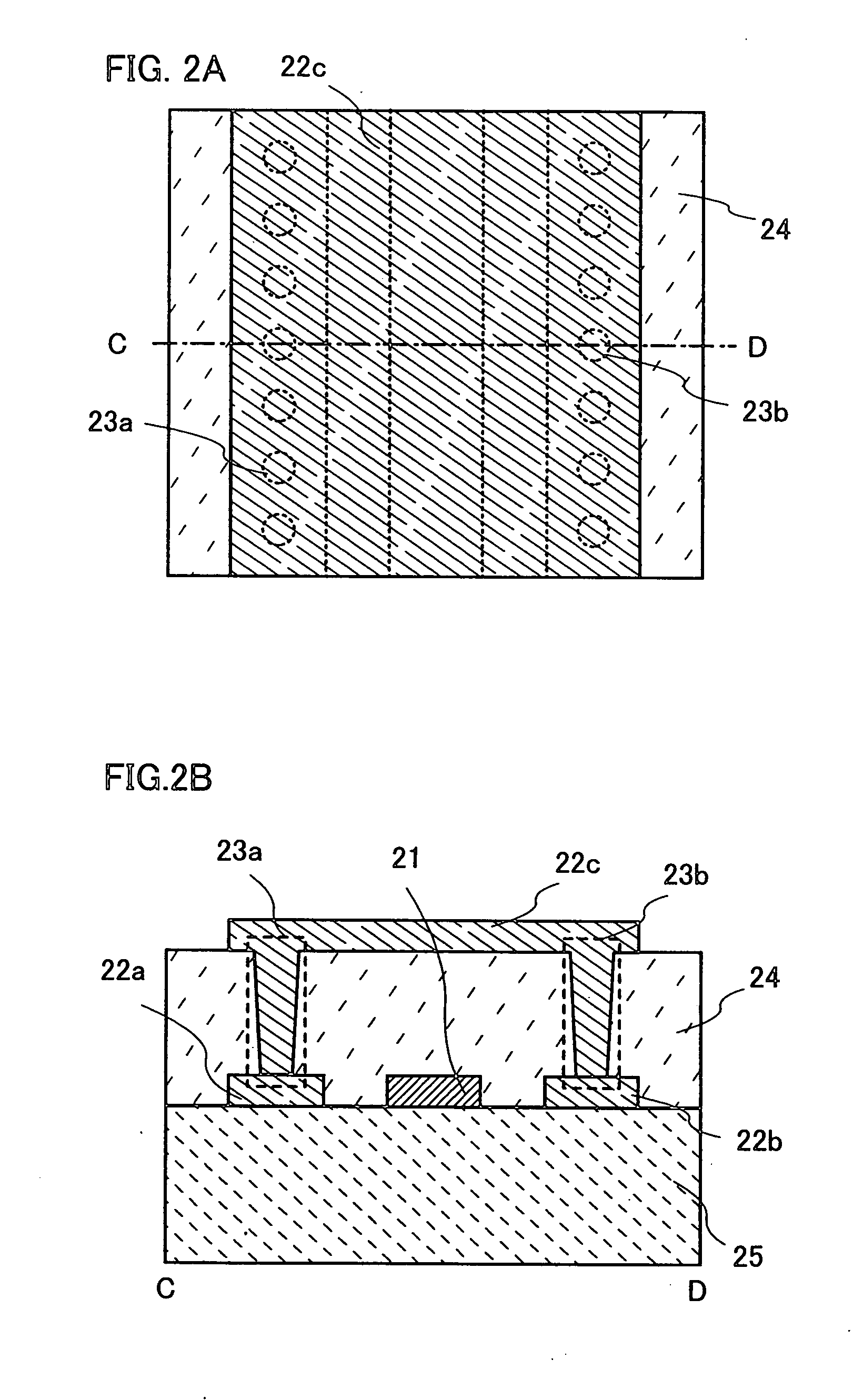
[0043]FIG. 2A is a top view of a semiconductor device of this embodiment mode, and FIG. 2B is a cross sectional view along a line C-D. The semiconductor device of this embodiment mode has a signal wiring layer 21 for a signal received from or transmitted to an antenna, a conductive layer 22a, a conductive layer 22b, a conductive layer 22c, an insulating layer 24 including an opening 23a and an opening 23b, and an insulating layer 25. The conductive layer 22a, the conductive layer 22b, and the conductive layer 22c are referenced to a signal (e.g., radio frequency signal) received from or transmitted to the signal wiring layer, and are set to an arbitrary potential. The conductive layer 22a and the conductive layer 22b are connected to the conductive layer 22c with a plurality of vias (the opening 23a and the opening 23b) along the propagation direction...

embodiment mode 3

[0047] In this embodiment mode, an example of a semiconductor device of the invention is described with reference to FIGS. 3A and 3B.

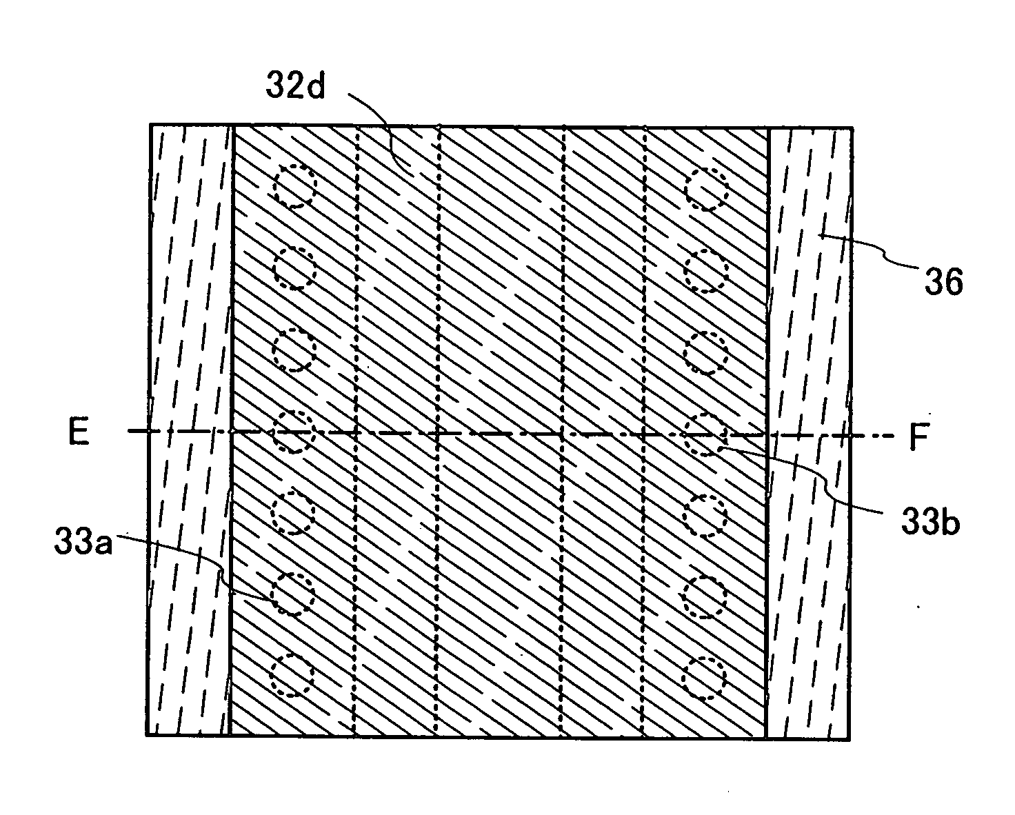
[0048]FIG. 3A is a top view of a semiconductor device of this embodiment mode, and FIG. 3B is a cross sectional view along a line E-F. The semiconductor device of this embodiment mode has a signal wiring layer 31 for a signal received from or transmitted to an antenna, a conductive layer 32a, a conductive layer 32b, a conductive layer 32c, a conductive layer 32d, an insulating layer 34 and an insulating layer 36 each including an opening 33a and an opening 33b, and an insulating layer 35. The conductive layer 32a, the conductive layer 32b, the conductive layer 32c, and the conductive layer 32d are referenced to a signal (e.g., radio frequency signal) received from or transmitted to the signal wiring layer, and are set to an arbitrary potential. The conductive layer 32a and the conductive layer 32b are connected to the conductive layer 32c and the cond...


PUM


Abstract

The invention provides a technology for manufacturing a higher performance and higher reliability semiconductor device at low cost and with high yield. The semiconductor device of the invention has a first conductive layer over a first insulating layer; a second insulating layer over the first conductive layer, which includes an opening extending to the first conductive layer; and a signal wiring layer for electrically connecting an integrated circuit portion to an antenna and a second conductive layer adjacent to the signal wiring layer, which are formed over the second insulating layer. The second conductive layer is in contact with the first conductive layer through the opening, and the first conductive layer overlaps the signal wiring layer with the second insulating layer interposed therebetween.

Description

BACKGROUND OF THE INVENTION [0001] 1. Field of the Invention [0002] The present invention relates to a semiconductor device and a manufacturing method of the same. [0003] 2. Description of the Related Art [0004] In recent years, identification technology where an ID (identification number) is assigned to each object so as to reveal data thereon such as the history has been attracting attention, which is utilized for production management and the like. Above all, semiconductor devices capable of communicating data without contact have been developed. Such semiconductor devices include an RFID (Radio Frequency Identification) tag (also called an ID tag, an IC tag, an IC chip, an RF (Radio Frequency) tag, a wireless tag, an electronic tag, or a wireless chip), and the like have been introduced into companies, markets and the like. [0005] Most of these semiconductor devices are constituted by an antenna and an integrated circuit. For example, an information storage component is mounted ...

Claims


Application Information

Patent Timeline
Patent Type & Authority Applications(United States)
IPC IPC(8): H01L23/52H01L23/48
CPCH01L23/5225H01L23/552H01L27/13H01L29/78624H01L29/78633H01L27/124H01L2924/12044H01L2924/3011H01L2924/0002H01L2223/6677H01L2924/00
Inventor MATSUZAKI, TAKANORI
Owner SEMICON ENERGY LAB CO LTD
Why Eureka
Try Eureka