A silicon capacitance microphone and its making method
A technology of silicon capacitors and microphones, applied in electret electrostatic transducers, electrostatic transducer microphones, etc., can solve problems such as difficult operation and limited production efficiency of silicon capacitor microphones, and achieve reduced overall thickness and good electromagnetic shielding Effects, Simple Effects
- Summary
- Abstract
- Description
- Claims
- Application Information
AI Technical Summary
Problems solved by technology
Method used
Image
Examples
Embodiment 1
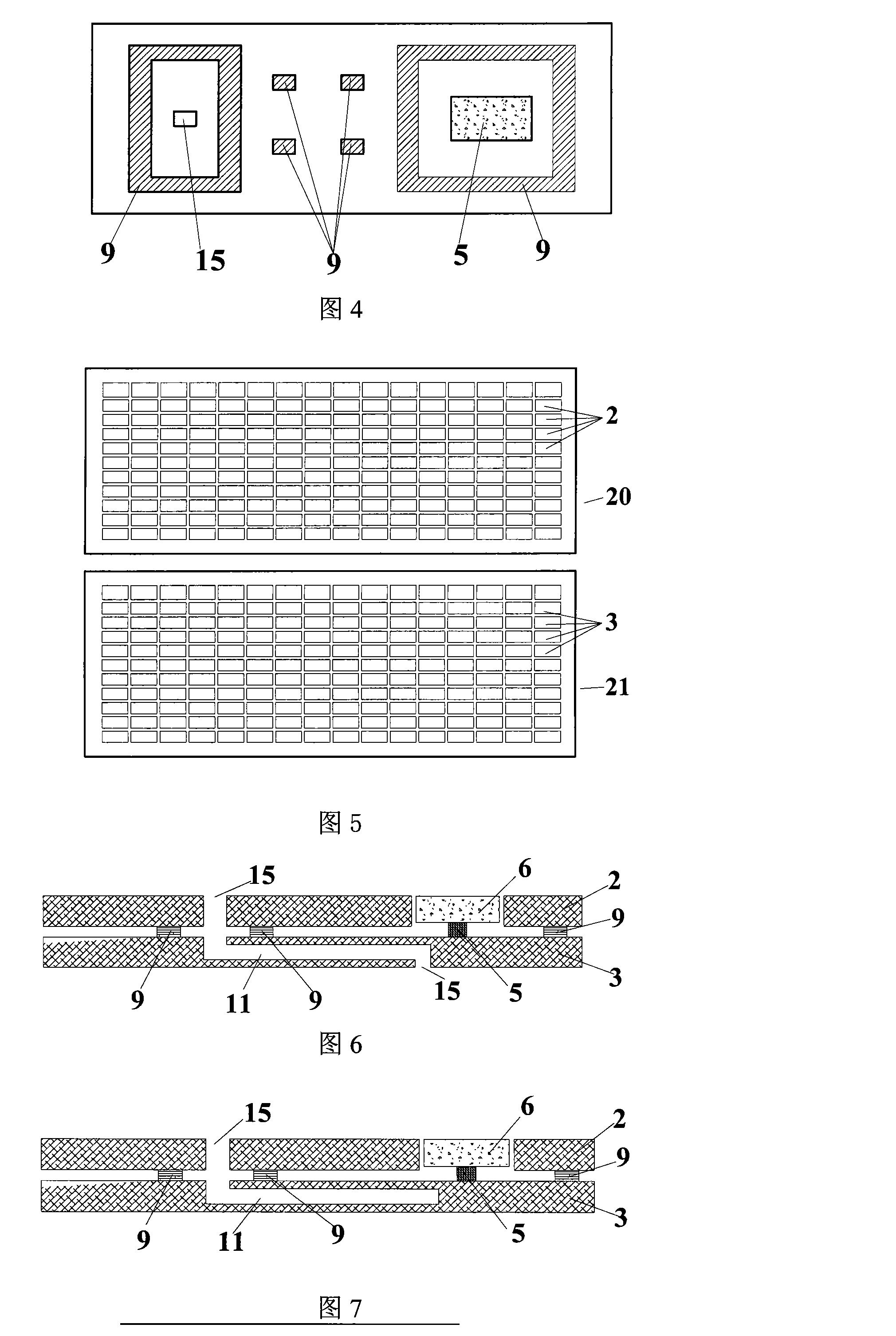
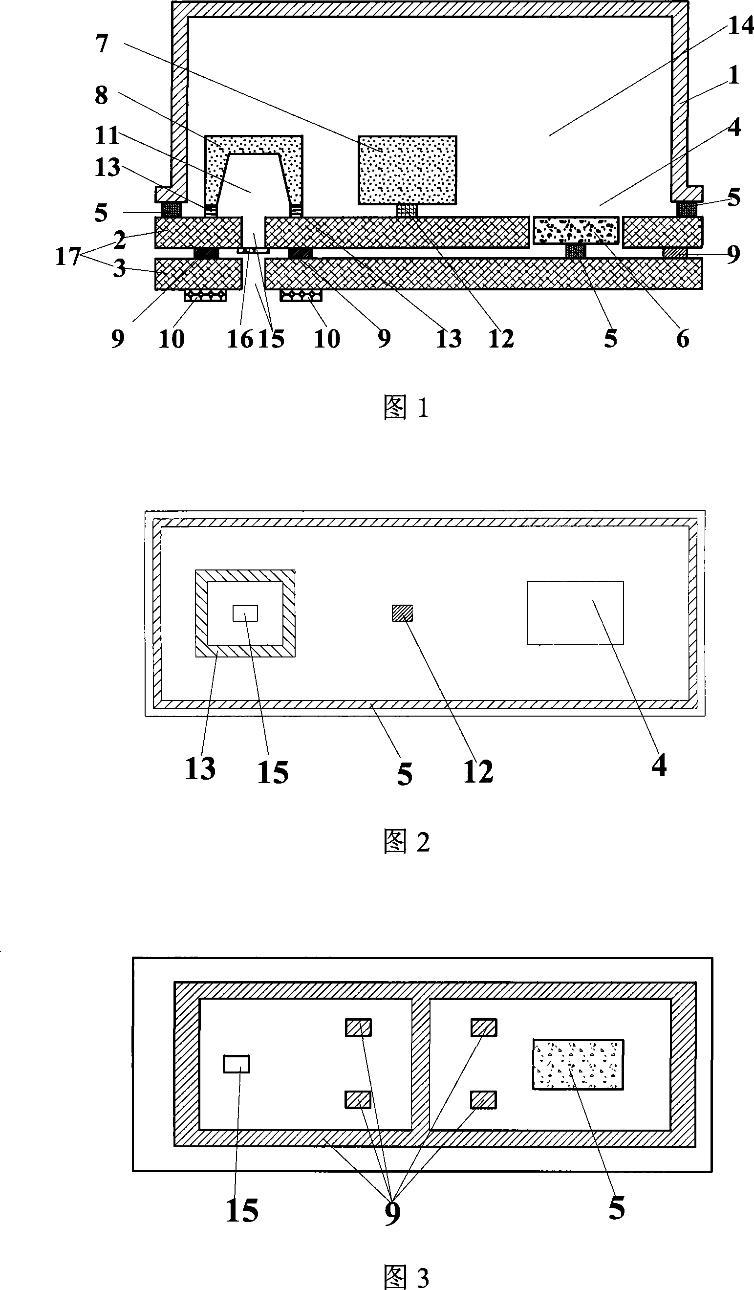
[0063] The silicon capacitive microphone of this specific embodiment, as shown in FIG. 1 , includes a housing 1 and a substrate assembly. The substrate assembly includes a substrate 17 and an acoustic sensor chip 8 , an IC device 7 and other passive devices 6 mounted on the substrate 17 . The edge of the housing 1 is fixed to the substrate 17 by conductive glue or solder paste 5 , and a cavity 14 is formed between the housing 1 and the substrate 17 .
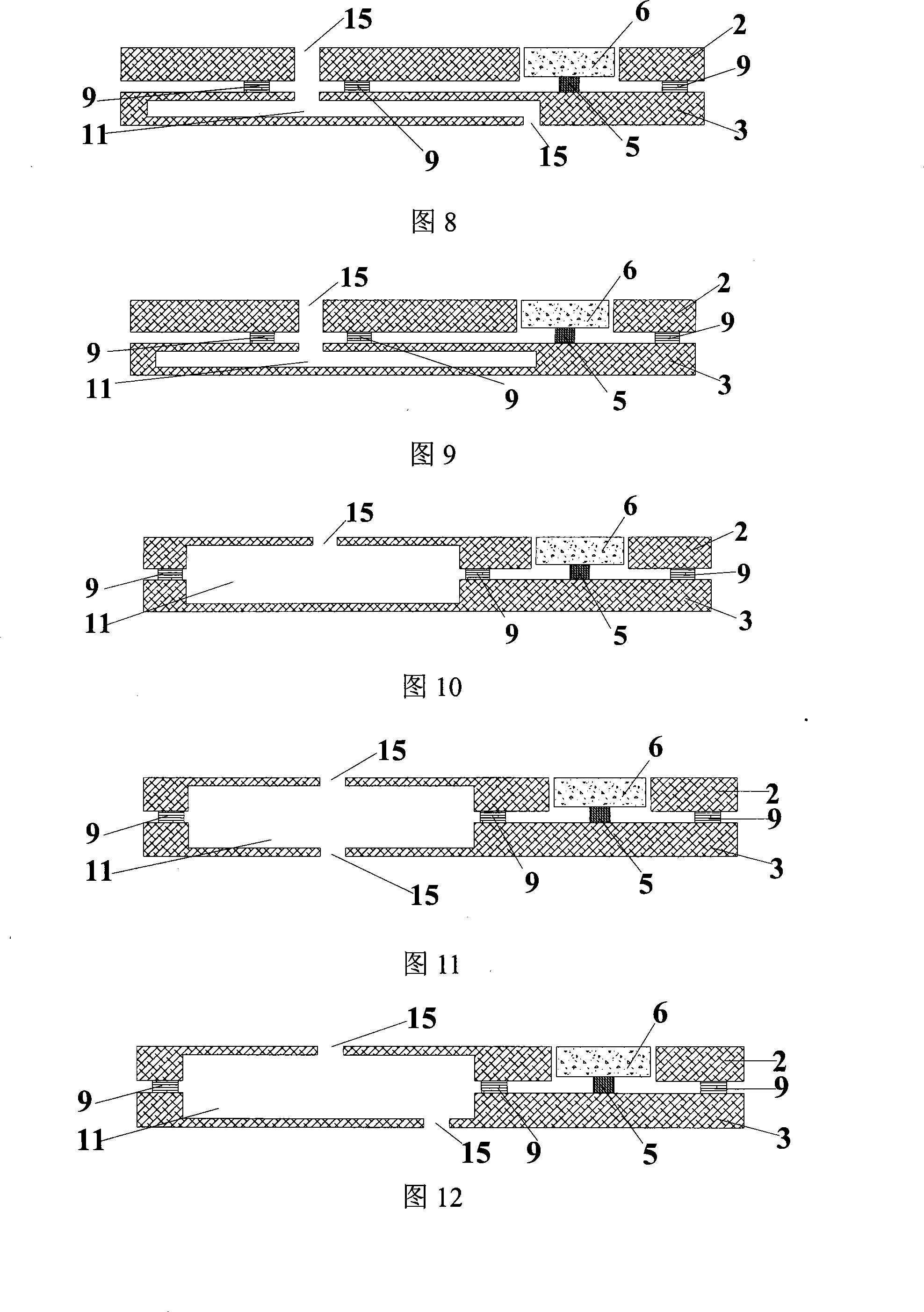
[0064] In the silicon condenser microphone of this embodiment, the substrate 17 includes an upper substrate 2 and a lower substrate 3 . The upper substrate 2 and the lower substrate 3 are fixed and electrically connected through the connection pad 9 .
[0065] The acoustic sensor chip 8 is located in the cavity 14 and bonded on the upper surface of the upper substrate 2 by the acoustic sensor adhesive 13 . The acoustic sensor chip 8 is electrically connected to the upper substrate 2 through a bonding process (the bonding line ...
Embodiment 2
[0097] The structure of the silicon capacitive microphone in this specific embodiment is shown in FIG. 13 . The difference from Embodiment 1 is that the output terminal pad 10 for connecting with the client circuit board is arranged on the upper surface of the upper substrate and is located at the periphery of the casing 1 . The advantage of this structure is that it can provide another way to connect with the client. The main body of the silicon condenser microphone can be accommodated in the hole dug on the circuit board of the client to meet the needs of the client. The scheme about expanding the acoustic cavity 11 in the first embodiment is also applicable to this embodiment.
[0098] The manufacturing method of the silicon capacitive microphone in this specific embodiment is almost the same as that in Embodiment 1, the only difference is that in the first step, the upper entire board 20 and the lower entire board 21 are fabricated by using printed circuit board technology...
Embodiment 3
[0100] The structure of the silicon capacitive microphone in this specific embodiment is shown in FIG. 14 . The difference from the first embodiment is that the acoustic sensor chip 8 and the IC device 7 are bonded on the upper surface of the lower substrate 3 and located in the receiving hole 4 opened on the upper substrate 2 . The acoustic sensor chip 8 and the IC device 7 are electrically connected to the lower substrate through bonding wires. Other passive components 6 are bonded on the upper substrate 2 through conductive glue or solder paste 5 and are electrically connected to the upper substrate 2 . Since the height of the acoustic sensor chip 8 and the IC device 7 is generally greater than that of other passive devices 6, the cavity 14 can accommodate the acoustic sensor chip 8 and the IC device 7, and the thickness of the substrate can be properly reduced. Therefore, the advantage of adopting this structure is that the overall height of the silicon condenser micropho...
PUM
 Abstract
Description
Claims
Application Information


