

Active matrix display circuit substrate, display panel including the same, inspection method thereof, and inspection device thereof
- Summary
- Abstract
- Description
- Claims
- Application Information
AI Technical Summary
Benefits of technology
Problems solved by technology
Method used
Image

Examples
Embodiment Construction
[0048] The active-matrix display circuit substrate, the display panel comprising the same, the inspection method thereof, and the inspection device thereof that are the preferred embodiments of the present invention will now be described in detail while referring to the attached drawings.
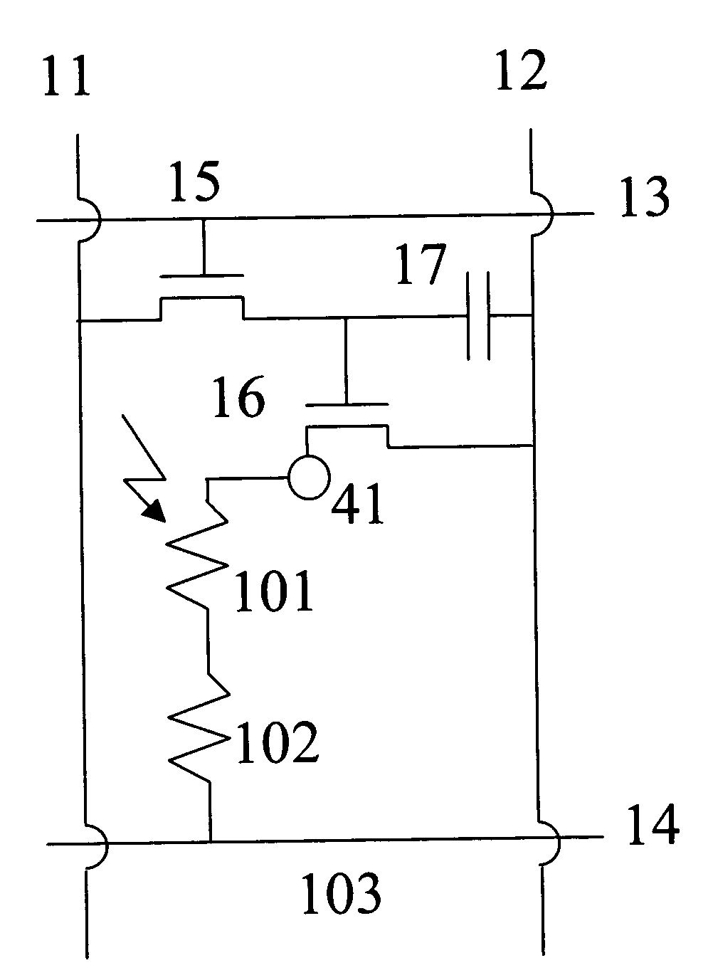
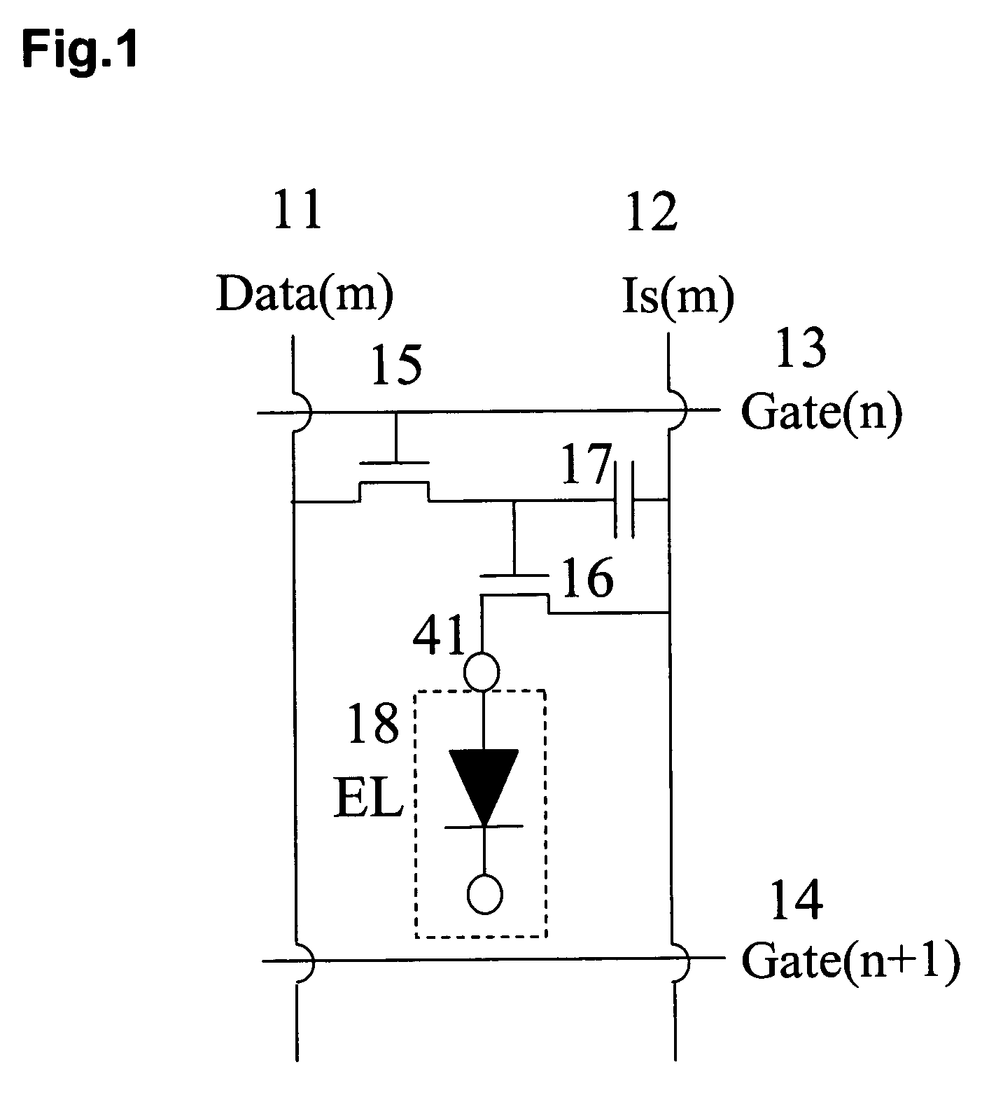
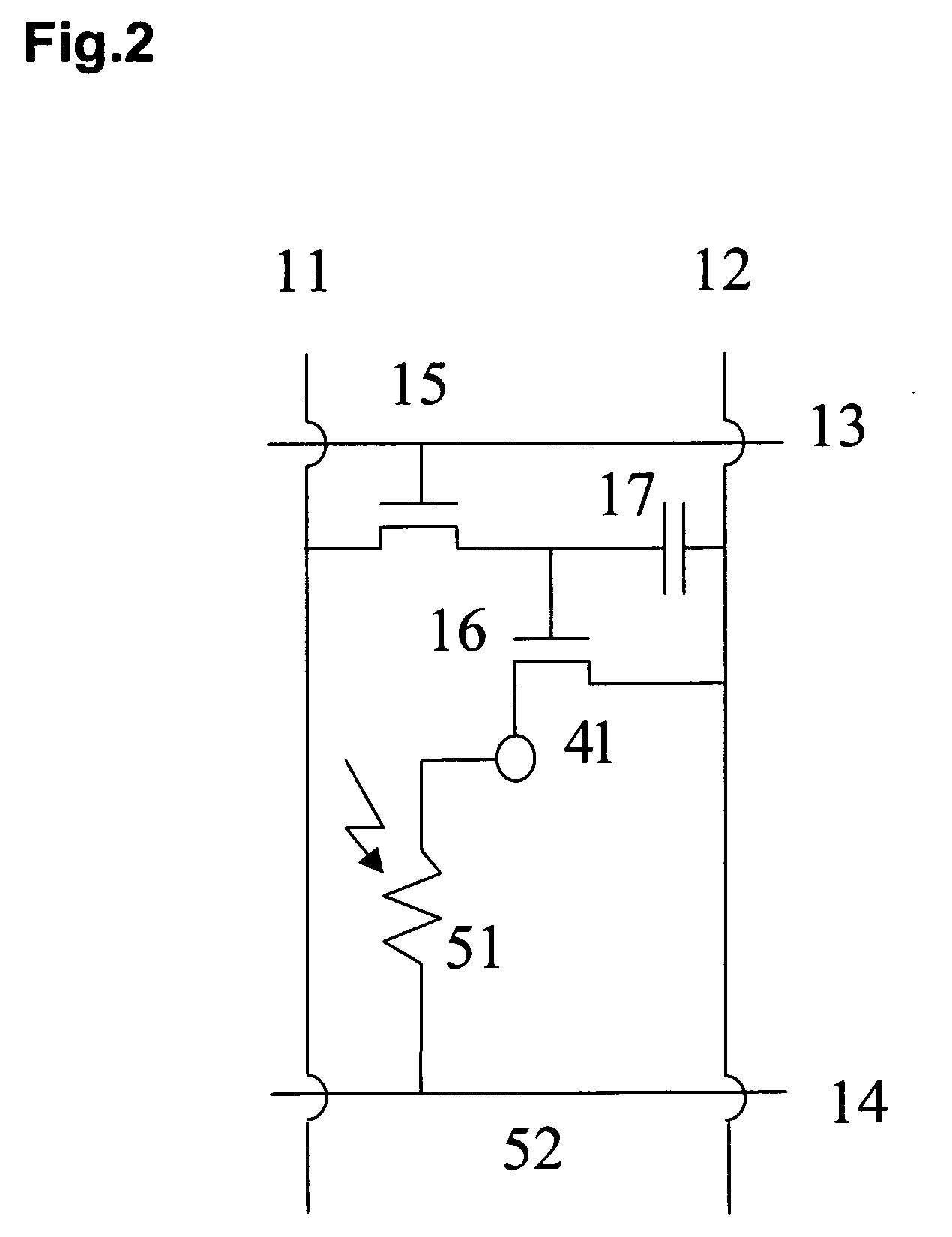
[0049]FIG. 1 is a drawing showing the structure of a TFT (thin-film transistor) active-matrix display circuit substrate for a typical organic EL display. The drawing shows a circuit corresponding to a single pixel. Wirings 11, 12, and 13 are the data line (m), the power line, and the gate line (n). These lines define the pixel units of the drive circuits of the display. TFT (thin-film transistors) 15 and 16 and a capacitor 17 are disposed for each pixel unit. As shown in the figure, EL material 18 is applied over an electrode 41 that is positioned in front of the drain of the thin-film transistor of the circuit and formed along the substrate surface. That is, EL material 18 is made such that light ...
PUM
 Abstract
Description
Claims
Application Information