Apparatus for ESD protection

a technology of electrostatic discharge and protective circuitry, applied in the direction of electrical apparatus, emergency protective arrangements for limiting excess voltage/current, transformers, etc., can solve the problems of esd damage, ics damage, and expensive product repairs

Inactive Publication Date: 2006-11-30
SARNOFF CORP +1
View PDF7 Cites 5 Cited by
  • Summary
  • Abstract
  • Description
  • Claims
  • Application Information

AI Technical Summary

Problems solved by technology

During installation of integrated circuits into products, these electrostatic discharges may destroy or impair the function of the ICs and thus require expensive repairs on the products, which could have been avoided by providing a mechanism for dissipation of the electrostatic discharge to which the IC may have been subjected.
That is, such protection circuitry is directly connected to a node of a circuit (i.e., semiconductor device or input pin of an IC) that may be susceptible to ESD damage.
Unfortunately, there are a number of disadvantages to such a design solution: (1) the ESD protection circuitry 102 creates a “footprint” (i.e., consumes additional area on an integrated circuit proximate each pad) that may not have been considered during the original circuit design, (2) the ESD protection circuitry introduces parasitic capacitance to the pad 110 (connection point between an IC and other circuit devices) and (3) the trigger circuit leaks current from the pad to ground where, in certain ICs, the leakage may interfere with normal operation of the protected circuitry and the overall IC.

Method used


Image

  • Apparatus for ESD protection
  • Apparatus for ESD protection
  • Apparatus for ESD protection

Examples


first embodiment

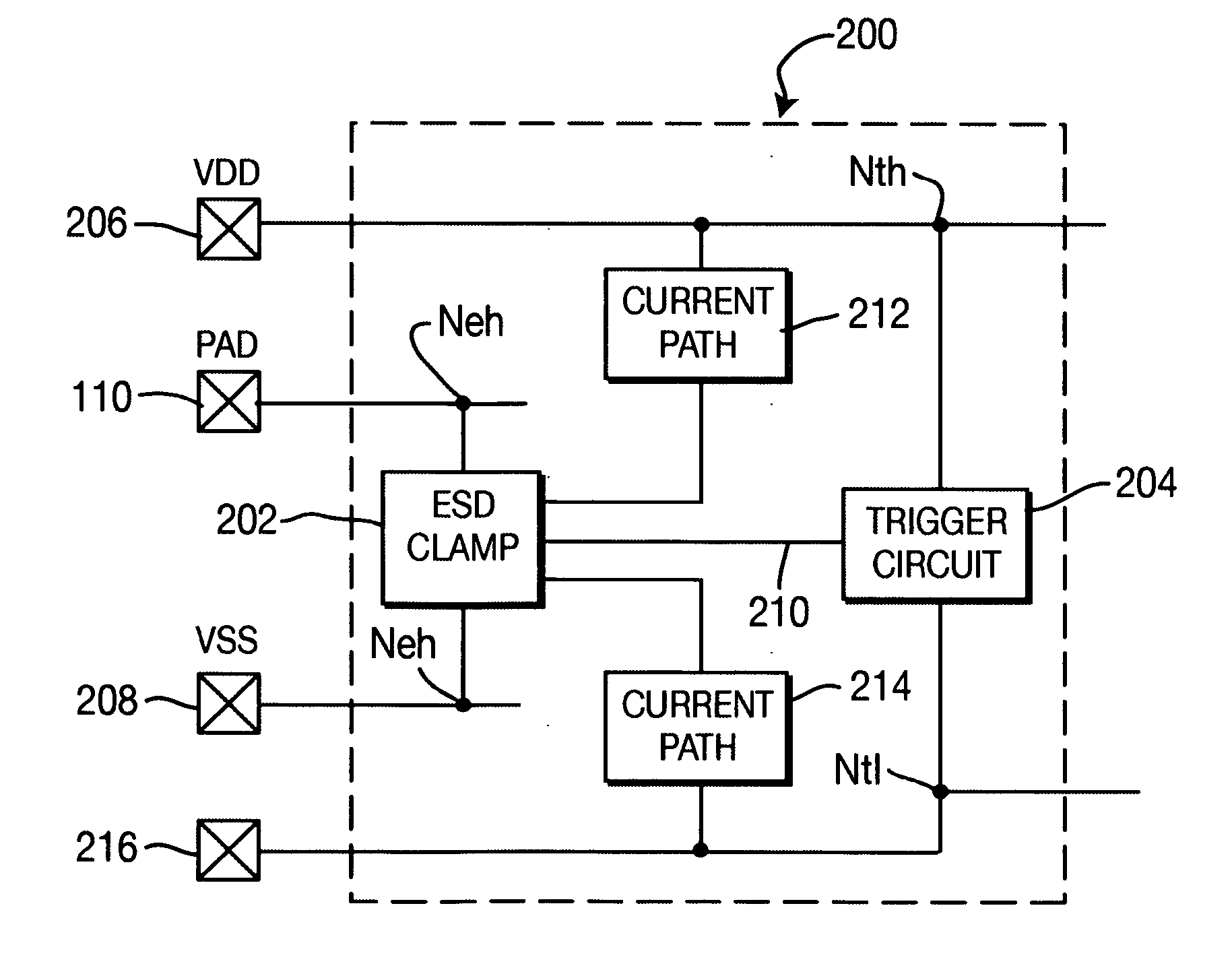
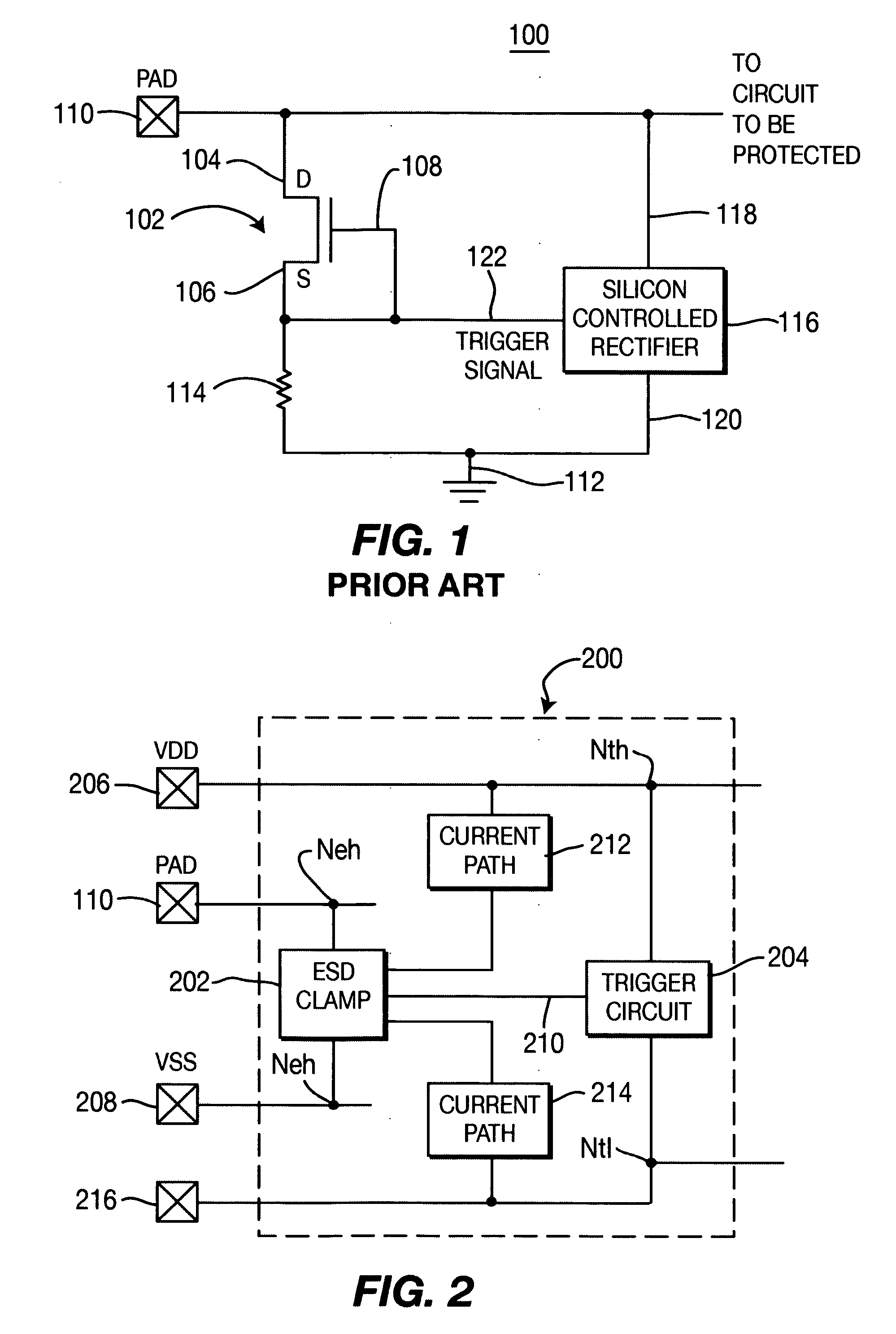
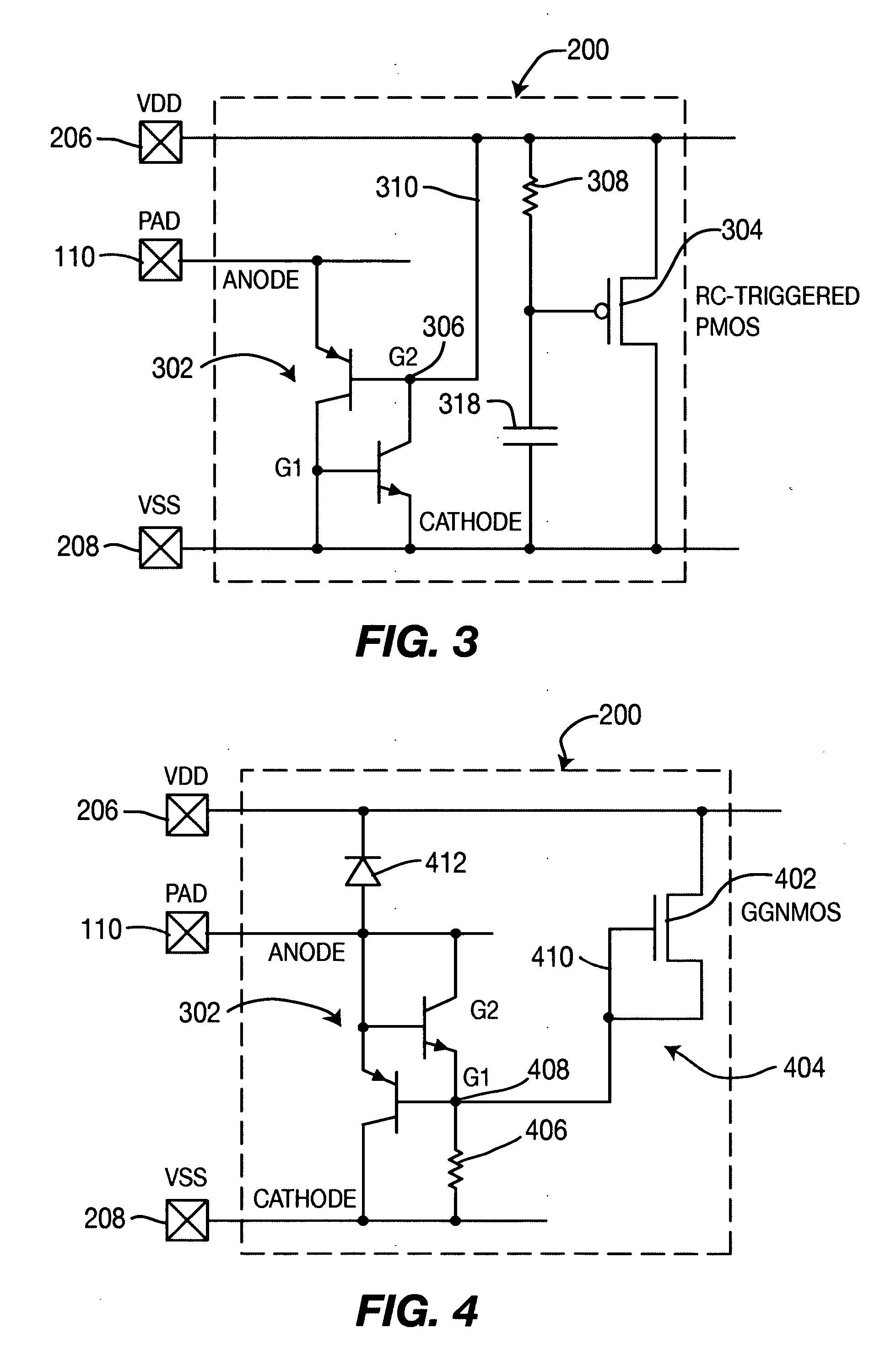
[0022]FIG. 3 depicts a circuit diagram of the invention, an ESDPC 200, as presented in FIG. 2. In this embodiment, implementation of the shunt subcircuit is accomplished by a silicon-controlled rectifier (SCR) 302. The SCR 302 is coupled between pad 110 (PAD=SCR Anode=Neh) and second voltage reference potential (VSS) 208 (SCR Cathode / G1=VSS=Nel). In this embodiment, current path 214 is a short that connects node 208 to node 216. A first base / collector node (G2) 306 is coupled to first voltage reference potential VDD. To trigger the SCR 302, a trigger circuit is added between VDD (Nth) and VSS (NtI). In one embodiment of the invention, the trigger circuit 204 of FIG. 2 is a PMOS 304 triggered by an RC circuit 308 / 310 connected thereto. Connection 310 between node 306 (G2) and VDD pad 206 acts as both a trigger connection 210 (FIG. 2) and conductive path between Neh and Nth (path 212 in FIG. 2).

[0023] In operation, a first current will flow from pad 110 through the Anode-G2 diode of t...

second embodiment

[0028]FIG. 4 depicts a circuit diagram of the invention, an ESDPC 200, as presented in FIG. 2. In this embodiment, implementation of the shunt subcircuit is again accomplished by an SCR 302. The SCR 302 is coupled between pad 110 and VSS (Anode / G2 coupled to PAD, Cathode coupled to VSS). A trigger circuit 404 is constructed between first voltage reference potential VDD 206 and second voltage reference potential VSS 208 as in the previous embodiments. However, trigger circuit 404 includes a GGNMOS 402 with a series resistor 406. A node 408 between the GGNMOS 402 and series resistor 406 is coupled to the G1 node (through path 410) of the SCR 302 to trigger the SCR 302 during ESD operation. Additionally, a diode 412 is connected between pad 110 and first voltage reference potential VDD 206. To reduce capacitance at the pad 110, the G2 node of the SCR 302 can be optionally coupled to first voltage reference potential VDD 206.

[0029] When an ESD event arrives at the pad 110, a first curre...


PUM


Abstract

Apparatus for ESD circuit protection including a trigger subcircuit coupled between a first voltage reference potential and second voltage reference potential and an ESD shunt subcircuit coupled to the trigger subcircuit between a circuit device to be ESD-protected and the second voltage reference potential. The ESD shunt subcircuit is adapted for connection by a pad of an integrated circuit (IC) connection. The ESD shunt subcircuit is a silicon-controlled rectifier (SCR) that has an anode connected to the circuit device to be ESD-protected and a cathode connected to the second voltage reference potential. The trigger subcircuit is either an RC-triggered PMOS or a GGNMOS and series connected resistor.

Description

[0001] This application claims benefit of U.S. provisional patent application Ser. No. 60 / 610,294, filed Sep. 16, 2004, which is incorporated by reference.BACKGROUND OF THE INVENTION [0002] 1. Field of the Invention [0003] This invention generally relates to the field of electrostatic discharge (ESD) protection circuitry and, more specifically, improvements for silicon controlled rectifier (SCR) structures in the protection circuitry of an integrated circuit (IC). [0004] 2. Description of the Related Art [0005] Integrated circuits (ICs) and other semiconductor devices are extremely sensitive to the high voltages that may be generated by contact with an ESD event. As such, electrostatic discharge (ESD) protection circuitry is essential for integrated circuits. An ESD event commonly results from the discharge of a high voltage potential (typically, several kilovolts) and leads to pulses of high current (several amperes) of a short duration (typically, 100 nanoseconds). An ESD event is...

Claims


Application Information

Patent Timeline
Patent Type & Authority Applications(United States)
IPC IPC(8): H02H9/00
CPCH01L27/0262
Inventor CAMP, BENJAMIN VANKEPPENS, BART
Owner SARNOFF CORP
Why Eureka
Try Eureka