Piping system structure of semiconductor equipment

Inactive Publication Date: 2006-12-07
MACRONIX INT CO LTD
View PDF3 Cites 4 Cited by
  • Summary
  • Abstract
  • Description
  • Claims
  • Application Information

AI Technical Summary

Benefits of technology

[0010] Accordingly, the present invention is directed to a piping system structure of semiconductor equipment. The piping system structure enhances the throughput of the semiconductor process.
[0011] The present invention is directed to a piping system structure of semiconductor equipment. The piping system structure reduces the size of the semiconductor equipment.
[0018] Accordingly, the pneumatic pump of the present invention can effectively reduce the size of the semiconductor equipment. The process throughput is also increased. Since the sensors at the pump of the present invention sense the position of the valve of the pump, whether the operation of the pump is normal can be determined according to the position of the valve of the pump. If the operation of the pump is abnormal, a warning message is generated and outputted to inform operators.

Problems solved by technology

Since the operation of the stepping motor in the electrical pump is slow, it affects the operating efficiency of the photoresist coater.
Due to the large size of an electrical pump, the photoresist coater occupies a lot of space as well.

Method used


Image

  • Piping system structure of semiconductor equipment
  • Piping system structure of semiconductor equipment
  • Piping system structure of semiconductor equipment

Examples


Embodiment Construction

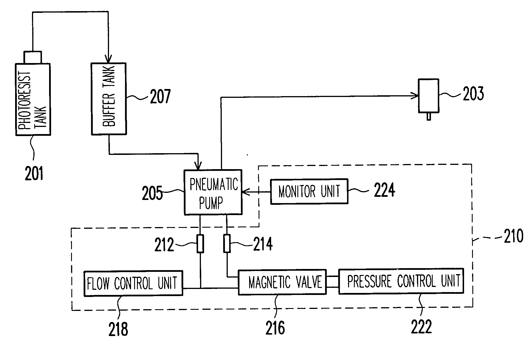
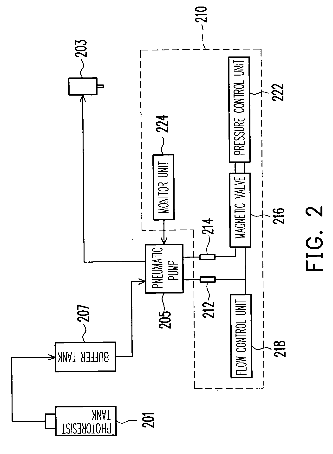
[0023]FIG. 2 is a schematic drawing showing a piping system structure of semiconductor equipment according to a preferred embodiment of the present invention. Referring to FIG. 2, the semiconductor equipment is adapted to dispense a fluid material stored in the vessel 201 on a wafer (not shown) through the nozzle 203. The dispensing process can be performed by pumping the fluid material stored in the vessel 201 to the nozzle 203 through the pneumatic pump 205.

[0024] In this embodiment, the semiconductor equipment described above can be a photoresist coater. The vessel 201 can be a photoresist tank. The fluid material can be photoresist. To simplify the interpretation and let one of ordinary skill in the art understand the present invention, a photoresist coater is used as the exemplary embodiment of the present invention. One of ordinary skill in the art knows that the scope of the present invention is not limited to the photoresist coater.

[0025] When a photoresist coating process...


PUM


Abstract

A piping system structure of semiconductor equipment comprises a vessel, a nozzle and a pneumatic pump. The pneumatic pump drains a fluid material in the vessel and transmits the fluid material to the nozzle to spray on the wafer. The piping system structure further comprises a first sensor, a second sensor and a processor. Wherein, the first sensor and the second sensor are disposed at the pneumatic pump to sense whether a valve in the pneumatic pump is at a first position or at a second position and generate a first sensing signal and a second sensing signal to the processor, respectively. When the difference between the time of receiving the first sensing signal and the time of receiving the second sensing signal exceeds a preset value, the processor determines that the operation of the pump is abnormal. Then, the processor controls the semiconductor equipment to generate a warning message.

Description

BACKGROUND OF THE INVENTION [0001] 1. Field of the Invention [0002] The present invention relates to a piping system structure, and more particularly, to a piping system structure of semiconductor equipment. [0003] 2. Description of the Related Art [0004] Various liquids are used in different processes in semiconductor fabrication. For example, a photoresist (PR) is used in a coating process in which the photoresist is sprayed on the wafer for a subsequent lithographic process. [0005]FIG. 1 is a schematic drawing showing a prior art piping system structure of a photoresist coater. The photoresist coater is adapted for a photoresist coating process to uniformly spray the photoresist on the wafer. Referring to FIG. 1, the prior art piping system structure of the photoresist coater comprises the photoresist tank 101, the buffer tank 103, the nozzle 105 and the electrical pump 110. Wherein, the electrical pump 110, such as a CYBOR pump, pumps the photoresist stored in the photoresist ta...

Claims


Application Information

Patent Timeline
IPC IPC(8): B05C11/00
CPCB05B12/006H01L21/67253H01L21/67242H01L21/6715
Inventor HUANG, CHAIN-CHIPENG, TSUNG-HANWANG, CHING-HUIWANG, SUE-PENG
Owner MACRONIX INT CO LTD
Why Eureka
Try Eureka