High power LED package and fabrication method thereof

Inactive Publication Date: 2006-12-07
SAMSUNG ELECTRONICS CO LTD
View PDF12 Cites 53 Cited by
  • Summary
  • Abstract
  • Description
  • Claims
  • Application Information

AI Technical Summary

Benefits of technology

[0024] The present invention has been made to solve the foregoing problems of the prior art and therefore an object of certain embodiments of the present invention is

Problems solved by technology

Thus, with high level of power consumption, the LED typically adopts a heat connecting structure to prevent the semiconductor device and the package itself from being damaged from the heat generated during the emission of light.
However, the conventional LED package 10 having such a structure entails a process of forming an assembly hole 15a and inserting the heat connecting structure 12 into the center of the molded part 15 through the assembly hole 15a. Therefore, the assembly structure and process is too complicated to be fully automated, lowering productivity.
In addition, the package disadvantageously has a large volume.
This as a result degrades the degree of freedom in lens design.
Thus, this LED package type is not suitable for an illumination light source that is required to uniformly light a wide area by optimally using the unique beam ang

Method used


Image

  • High power LED package and fabrication method thereof
  • High power LED package and fabrication method thereof
  • High power LED package and fabrication method thereof

Examples


Embodiment Construction

[0066] The present invention will now be described more fully hereinafter with reference to the accompanying drawings, in which preferred embodiments of the invention are shown.

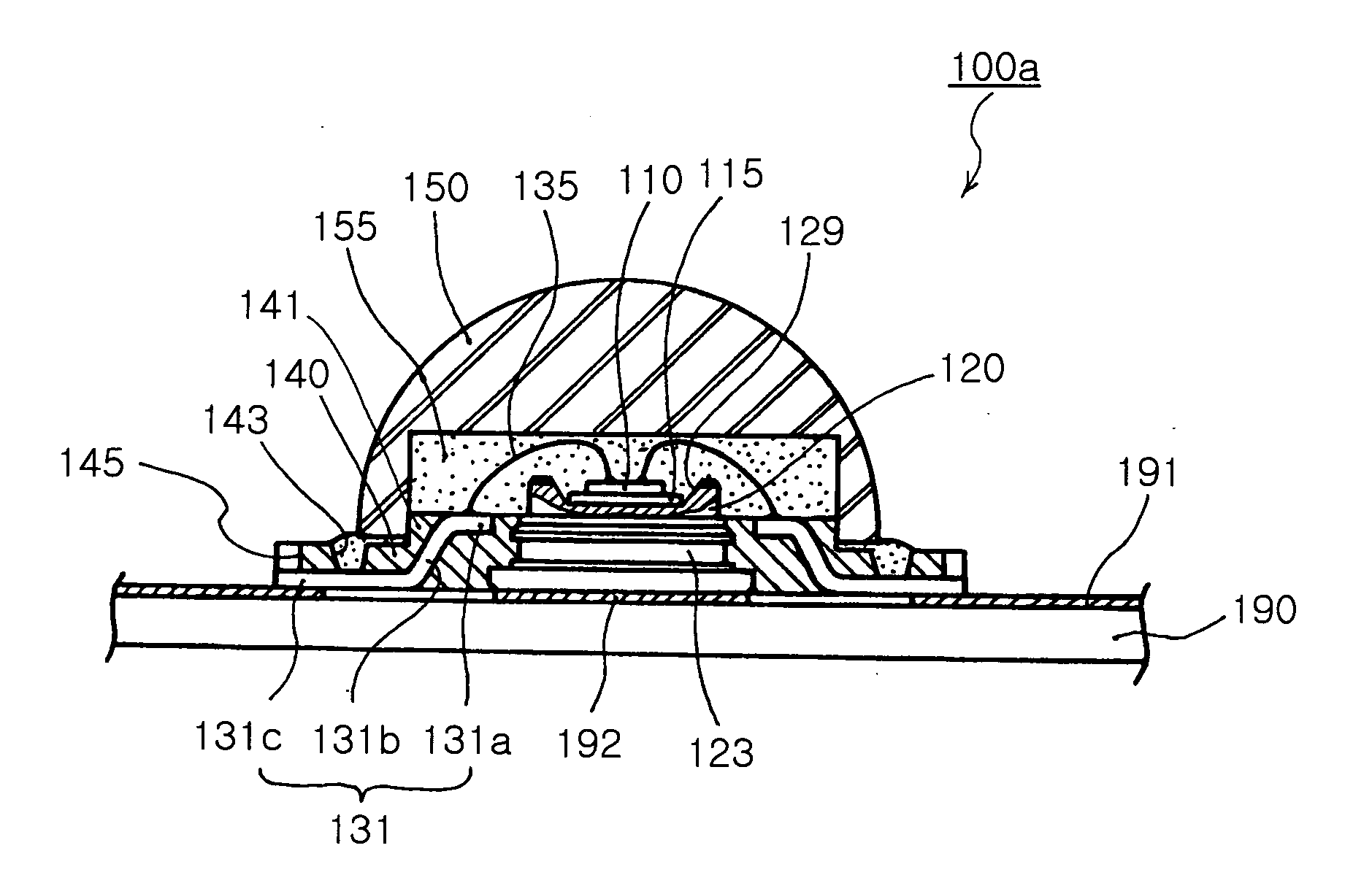
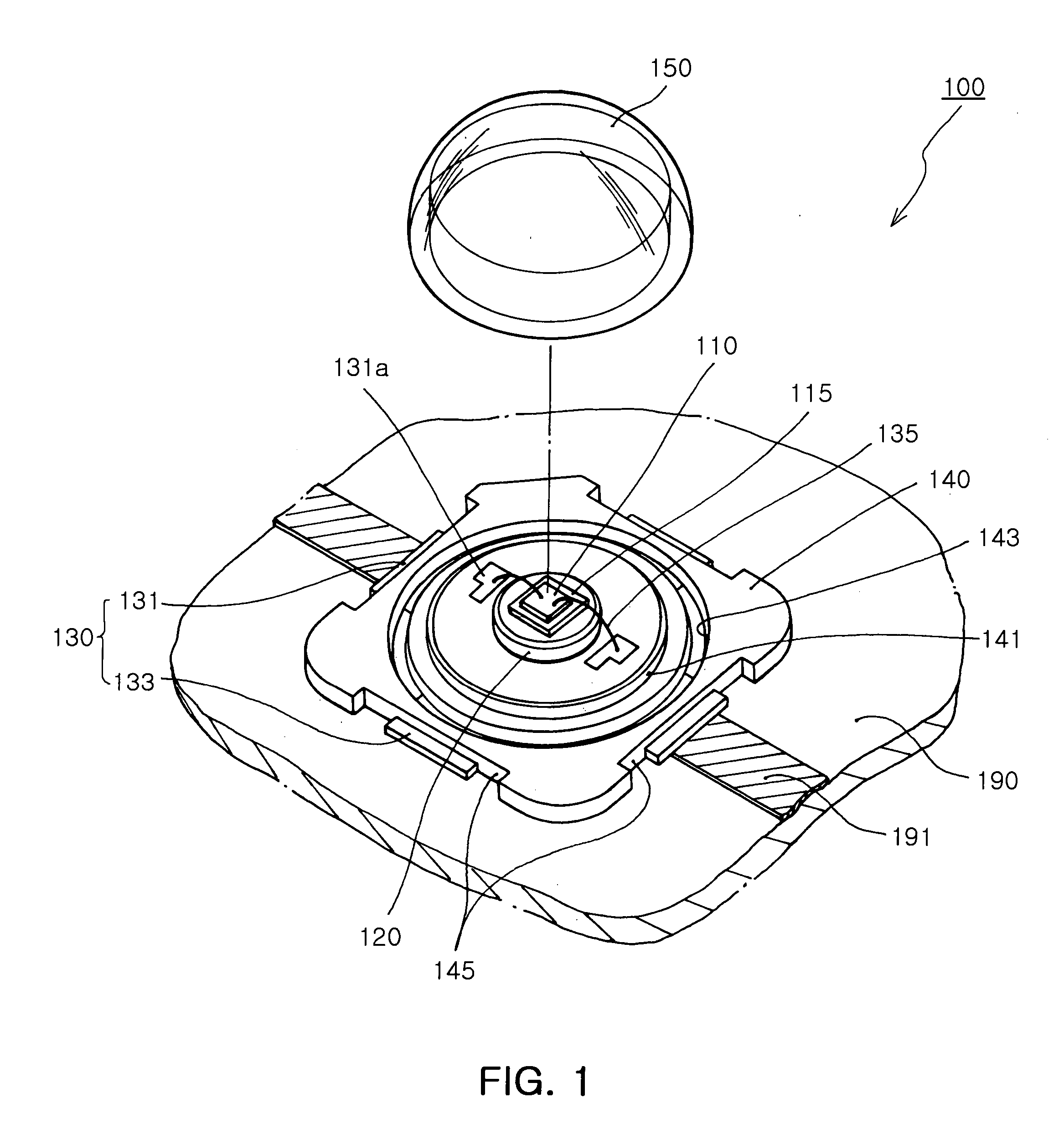
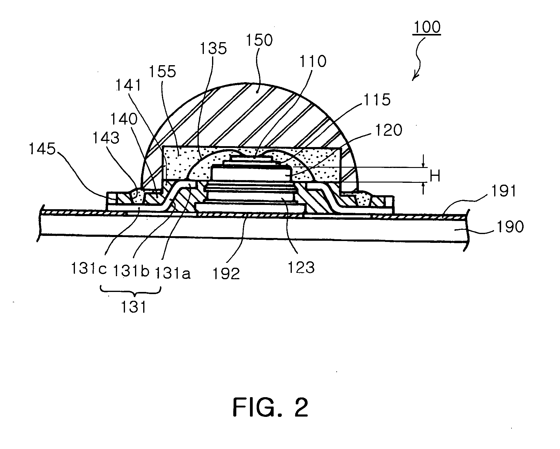
[0067] As shown in FIGS. 1 and 2, an LED package 100 according to an embodiment of the invention is designed to dispose a light source, which emits light in response to current applied, above the upper surface of a molded part in order to optimize the unique beam angle of the light source, thereby maximizing Lighting efficiency. The LED package 100 includes a light emitting part 110, a heat connecting part 120, frames 130 and a molded part 140.

[0068] The light emitting part 110 is at least one LED that is a semiconductor device for generating light accompanied with heat when current flows through it.

[0069] Such an LED is composed of an active layer and cladding layers formed on both sides of the active layer, and can be made of but not limited to various semiconductor materials such as GaAlAs, AlGaIn used ...


PUM


Abstract

An LED diode package includes a heat connecting part for mounting a light emitting part on an upper surface thereof, frames electrically connected to the light emitting part while holding the heat connecting part and a molded part fixing the heat connecting part and the frames together. The light emitting part generates light in response to current applied thereto, and the upper surface of the heat connecting part is protruded beyond an upper surface of the molded part to a predetermined height. This can optimize the unique beam angle of the light source thereby to maximize lighting efficiency as well as prevent overflow of the encapsulating material in the assembling process of the lens, which may otherwise soil adjacent components.

Description

RELATED APPLICATION [0001] The present application is based on and claims priority from Korean Application Number 10-2005-0047782, filed Jun. 3, 2005, the disclosure of which is hereby incorporated by reference herein in its entirety. BACKGROUND OF THE INVENTION [0002] 1. Field of the Invention [0003] The present invention relates to a high power LED package and a fabrication method thereof, more particularly, in which a molded part that integrally fixes frames together with a heat connecting part, and a light source is disposed above the upper surface of the molded part to optimally utilize unique beam angle thereof, thereby maximizing light efficiency. [0004] 2. Description of the Related Art [0005] In general, an LED (Light Emitting Diode) is a semiconductor device generating light when current flows through it, and is provided in the form of a PN junction diode made of for example GaAs or GaN optical semiconductor that converts electric energy into light energy. [0006] The light...

Claims


Application Information

Patent Timeline
IPC IPC(8): H01L33/00H01L33/56H01L33/58H01L33/62H01L33/64
CPCH01L33/486H01L33/58H01L33/642H01L2224/48091H01L2924/00014
Inventor LEE, SEON GOOHAHM, HUN JOOPARK, JUNG KYUHAN, KYUNG TAEGHAN, SEONG YEONKIM, DAE YEONPARK, YOUNG SAM
Owner SAMSUNG ELECTRONICS CO LTD
Why Eureka
Try Eureka