MOSFET using gate work function engineering for switching applications

Inactive Publication Date: 2006-12-07
ALPHA & OMEGA SEMICON LTD
View PDF6 Cites 34 Cited by
  • Summary
  • Abstract
  • Description
  • Claims
  • Application Information

AI Technical Summary

Benefits of technology

[0011] Specifically, it is an object of the present invention to provide an improved MOSFET device with a higher gate work function by implementing a P-doped gate in an N-MOSFET device. The P-type gate increases the threshold voltage and shifts the C-Vds characteristics. The reduced Cgd thus achieves the purpose of suppressing the shoot through and resolve the difficulties discussed above. Unlike the conventional techniques as shown in FIGS. 5 and 6, the reduction of the capacitance Cgd is achieved without requiring complicated fabrication processes and control of the recess electrode.
[0012] Briefly in a preferred embodiment this invention discloses a metal oxide semiconductor field effect transistor (MOSFET) device. The MOSFET device further includes a trenched gate filled with a material for adjusting a gate work function to increase an absolute value of threshold and to lower a gate drain capacitance Cgd. In a preferred embodiment, the MOSFET device includes a trenched gate filled with a gate material having a work function higher than an N+ poly for a n-channel MOSFET and lower than a P+ poly for a P-channel MOSFET. In another preferred embodiment, the MOSFET is a N-channel MOSFET and the trenched gate is filled with a P-doped gate material. In another preferred embod

Problems solved by technology

Conventional power MOSFET devices still face the shoot through problems that result in excessive dissipation and efficiency loss.
The shoot through condition results in excessive dissipation and efficiency loss.
However, large rate of change of the voltage over Q2 when Q2 is turned on may force Q4 to turn on as described above and cause shoot-through.
However, this solution will lead to excessive gate charge losses in th

Method used


Image

  • MOSFET using gate work function engineering for switching applications
  • MOSFET using gate work function engineering for switching applications
  • MOSFET using gate work function engineering for switching applications

Examples


Example

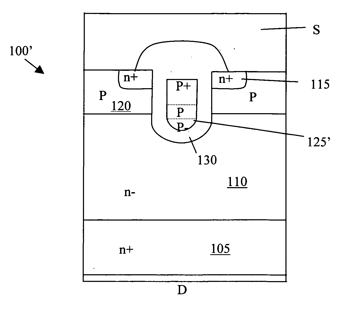
[0031] Referring to FIG. 7A for a side cross sectional view of a new n-channel MOSFET cell 100 of this invention. The MOSFET 100 is formed on an N+ substrate 105 functioning as a drain. The N+ substrate supporting an N− epi-layer 110 thereon to form a vertical pn-junction region with an N+ source region 115 formed on top of a deeper p-body region 120. The MOSFET 100 further includes a gate 125 formed with polysilicon layer deposited in a trench formed in the epi-layer 110 with a gate oxide layer 130 insulating the gate 125 inside the trench. A current path is established from the source 115 via a channel formed in the p-body 120 along the gate 125 and extends to the drain in the N+ substrate 105. In this new MOSFET cell 100, the work function of the gate is changed to create a shift in the C-V characteristic. To achieve the change of the work function of the gate 125, the gate 125 is doped with a p-type dopant to form a p-type gate.

[0032] With a p-type gate as shown in FIG. 7A, the...


PUM


Abstract

This invention discloses a new MOSFET device. The MOSFET device has an improved operation characteristic achieved by manufacturing a MOSFET with a higher gate work function by implementing a P-doped gate in an N-MOSFET device. The P-type gate increases the threshold voltage and shifts the C-Vds characteristics. The reduced Cgd thus achieves the purpose of suppressing the shoot through and resolve the difficulties discussed above. Unlike the conventional techniques, the reduction of the capacitance Cgd is achieved without requiring complicated fabrication processes and control of the recess electrode.

Description

BACKGROUND OF THE INVENTION [0001] 1. Field of the Invention [0002] The invention disclosed herein relates generally to the circuit configuration and packaging configuration of power MOSFETs. More particularly, this invention relates to a novel device for preventing shoot through problem by adjusting the work function of the MOS gate. [0003] 2. Description of the Prior Art [0004] Conventional power MOSFET devices still face the shoot through problems that result in excessive dissipation and efficiency loss. Referring to FIG. 1 for a circuit diagram of a conventional buck converter 10 that includes a high side MOSFET 15 and a low side MOSFET 20 serially connected between an input terminal 25 having an input voltage represented by Vin and a ground terminal 30. The drain of the low side MOSFET 20 is connected to the source of the high side MOSFET 15 at a mid point 35 connecting to the load 40 through inductance L and capacitance C. When the buck converter 10 operates at high speed, a s...

Claims


Application Information

Patent Timeline
IPC IPC(8): H01L29/94
CPCH01L29/4916H01L29/4983H01L29/7813H01L29/7811H01L29/66734
Inventor BHALLA, ANUPLUI, SIK K.
Owner ALPHA & OMEGA SEMICON LTD
Why Eureka
Try Eureka