Amorphization/templated recrystallization method for hybrid orientation substrates

Inactive Publication Date: 2006-12-07
GLOBALFOUNDRIES INC
View PDF3 Cites 29 Cited by
  • Summary
  • Abstract
  • Description
  • Claims
  • Application Information

AI Technical Summary

Benefits of technology

[0014] The present invention provides an ATR method for forming low-defect density hybrid orientation substrates which avoids the problems of (i) corner defects in the ATR'd regions, and (ii) undesired orientation change of the non-ATR'd regions.
[0020] This process flow with STI formation after the amorphization and low-temperature recrystallization steps but before a defect removal anneal avoids the two problems described above: (i) corner defects where the ATR'd regions contact STI, and (ii) the conversion of non-ATR'd (original orientation) DSB layer regions to the substrate orientation during the high-temperature defect removal anneal. In a slightly more complicated variation of this process flow, the trenches of the STI regions are formed before the defect removal anneal and filled with a permanent dielectric after the defect removal anneal, thereby eliminating the requirement that the STI fill be able to survive the defect removal anneal. In both process flows, the borders of the ATR'd regions adjacent to non-ATR'd DSB regions may contain defects after the recrystallization anneal. However, this is not a problem because these defective edge regions are quite localized (typically having a width of only about half the DSB layer thickness) and would ordinarily be replaced by STI.

Problems solved by technology

However, this high temperature annealing is not expected to be effective in eliminating corner defects 99.
While more aggressive annealing (e.g., more than a few hours at temperatures higher than 1300° C.) might help to a limited degree, it is not a preferred option due to concerns about reaction and dissolution of oxide layers contained in the STI fill.
One could devise methods to repair corner defects 99, but none appear to be very practical.
However, the steps to do this are quite involved.
While solving the corner defect problem, the ATR-before-STI approach of FIGS. 4A-4E unfortunately gives rise to another problem: when the recrystallization and high temperature defect-removal anneals are performed before STI formation, the non-ATR'd Si regions (or islands) 20′ can “disappear” by converting to the orientation of the underlying substrate. FIG. 5D shows a cross section analogous to the one of FIG. 5C at early stages of this disappearance / conversion process (i.e., after a slow furnace ramp to 1250° C.).

Method used


Image

  • Amorphization/templated recrystallization method for hybrid orientation substrates
  • Amorphization/templated recrystallization method for hybrid orientation substrates
  • Amorphization/templated recrystallization method for hybrid orientation substrates

Examples


Embodiment Construction

[0035] The present invention will now be described in more detail by referring to the drawings that accompany the present application. In the accompanying drawings, like and corresponding elements are referred to by like reference numerals. It is also noted that the drawings of the present invention representing the structures during the various processing steps of the present invention are provided for illustrative purposes and are thus not drawn to scale.

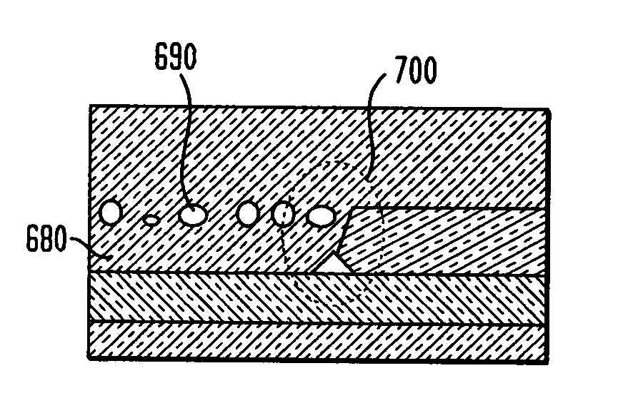
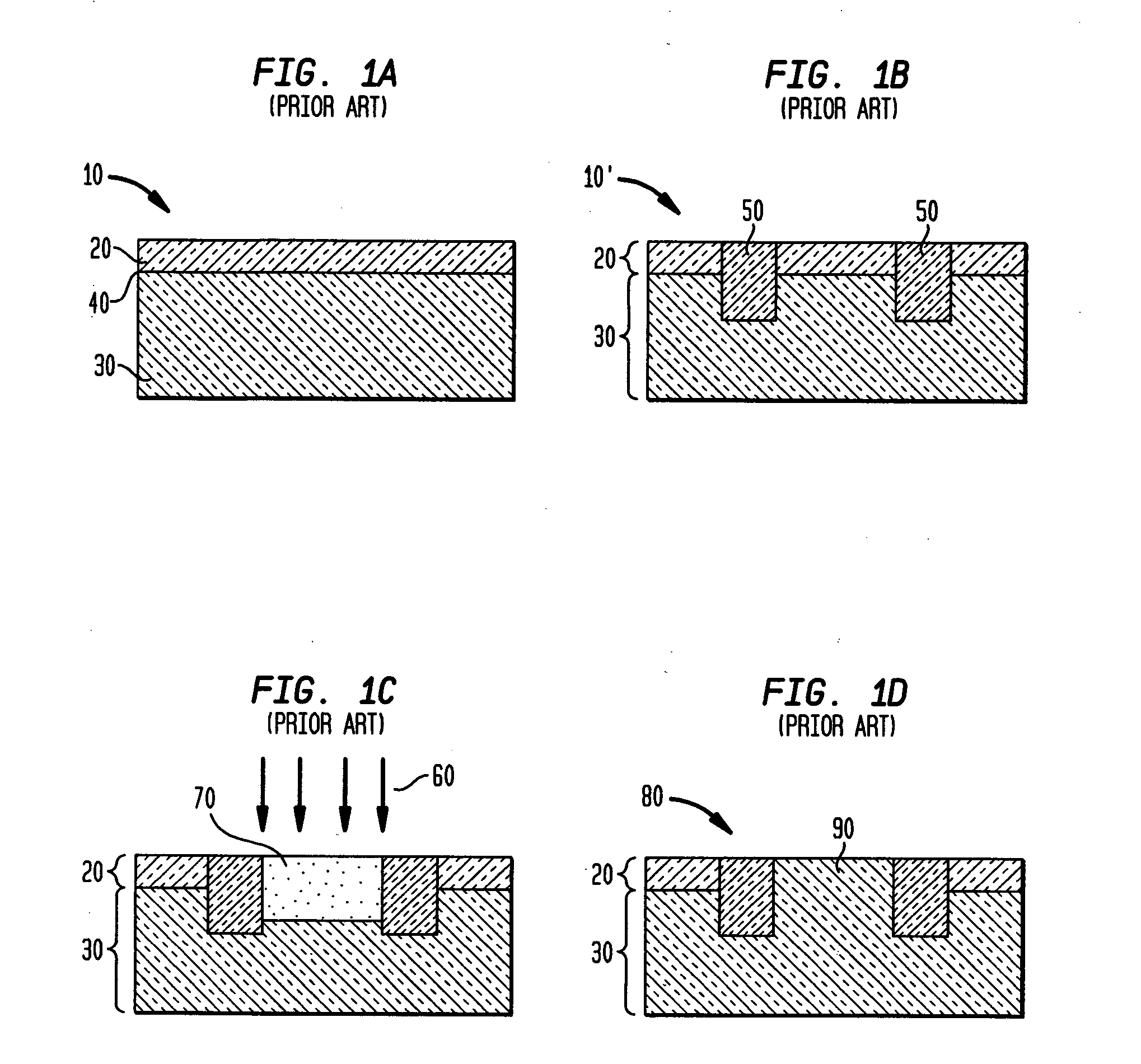
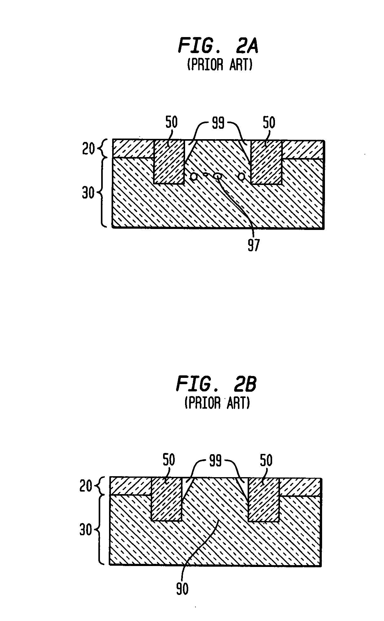
[0036] Reference is first made to FIGS. 6A-6E which are pictorial representations (through cross sectional views) illustrating the steps of a preferred embodiment of the inventive method for forming a low-defect density hybrid orientation substrate, i.e., a hybrid orientation substrate with no corner defects and a low (7 / cm2) concentration of residual end-of-range defects. FIG. 6A shows a starting substrate 200 comprising an upper silicon layer 220 having a first crystal orientation, a lower silicon layer or substrate 230 having ...


PUM


Abstract

The present invention provides an improved amorphization / templated recrystallization (ATR) method for fabricating low-defect-density hybrid orientation substrates. ATR methods for hybrid orientation substrate fabrication generally start with a Si layer having a first orientation bonded to a second Si layer or substrate having a second orientation. Selected regions of the first Si layer are amorphized and then recrystallized into the orientation of the second Si layer by using the second Si layer as a template. The process flow of the present invention solves two major difficulties not disclosed by prior art ATR methods: the creation of “corner defects” at the edges of amorphized Si regions bounded by trenches, and undesired orientation changes during a high temperature post-recrystallization defect-removal annealing of non-ATR'd regions not bounded by trenches. In particular, this invention provides a process flow comprising the steps of (i) amorphization and low-temperature recrystallization performed in substrate regions free of trenches, (ii) formation of trench isolation regions that subsume the defective regions at the edge of the ATR'd regions, and (iii) a high-temperature defect-removal anneal performed with the trench isolation regions in place.

Description

RELATED APPLICATIONS [0001] This application is related to U.S. patent application Ser. No. 11 / 031,142 entitled “Method for fabricating low-defect-density changed orientation Si,” filed Jan. 7, 2005, and to U.S. patent application Ser. No. 10 / 725,850, entitled “Planar substrate with selected semiconductor crystal orientations formed by localized amorphization and recrystallization of stacked template layers,” filed Dec. 2, 2003. The contents of each of the aforementioned U.S. patent applications are incorporated herein by reference in their entirety.FIELD OF THE INVENTION [0002] The present invention relates to crystalline substrate structures such as, for example, high-performance complementary metal oxide semiconductor (CMOS) circuits, in which carrier mobility is enhanced by utilizing different semiconductor surface orientations for p-channel field effect transistors (pFETs) and n-channel field effect transistors (nFETs). More particularly, the present invention relates to an imp...

Claims


Application Information

Patent Timeline
IPC IPC(8): H01L21/36
CPCH01L21/2022H01L21/823807H01L21/76224H01L21/02381H01L21/02433H01L21/02609H01L21/02532H01L21/02675
Inventor FOGEL, KEITH EDWARDSAENGER, KATHERINE L.SUNG, CHUN-YUNGYIN, HAIZHOU
Owner GLOBALFOUNDRIES INC
Why Eureka
Try Eureka