Fabrication of electronic devices using sacrificial seed layers

a technology of electronic devices and seed layers, applied in semiconductor devices, single crystal growth, chemistry apparatus and processes, etc., can solve problems such as current leakage, significant defect generation in semiconductor films, and defects negatively affecting device performance, so as to improve device performance, reduce defects, and remove the defect region

Active Publication Date: 2022-04-12
TEXAS A&M UNIVERSITY
View PDF6 Cites 0 Cited by
  • Summary
  • Abstract
  • Description
  • Claims
  • Application Information

AI Technical Summary

Benefits of technology

[0004]In an exemplary embodiment, the disclosure relates to a manufacturing process to remove or isolate defect regions of a semiconductor material to enhance device performance. Standard techniques, such as selective area epitaxy, are used to control where crystal growth takes place by patterning an opening in a dielectric. A semiconductor film is grown from the opening in the dielectric and extends over the dielectric mask. The portion of the semiconductor film grown over the mask has significantly less defects as compared to the semiconductor film grown directly above the window. The methods of this disclosure remove the defect region or reduce the amount of defects in the semiconductor film above the window to provide improvements in device fabrication procedures and device electrical performance.
[0005]The methods of the disclosure can be applied to integrated or discrete electronic devices to improve device performance. The process can be combined with current technology to improve device performance, yield, and reliability.

Problems solved by technology

Deposition (epitaxial growth) of a semiconductor material on a foreign substrate can result in significant defect generation in the semiconductor film due to mismatch in crystal spacing and thermal properties.
Defects negatively impact device performance.
For example, defects can cause current leakage, lower the breakdown voltage, and change the behavior of the device in the on-state due to electrons becoming trapped.

Method used


Image

  • Fabrication of electronic devices using sacrificial seed layers

Examples


Embodiment Construction

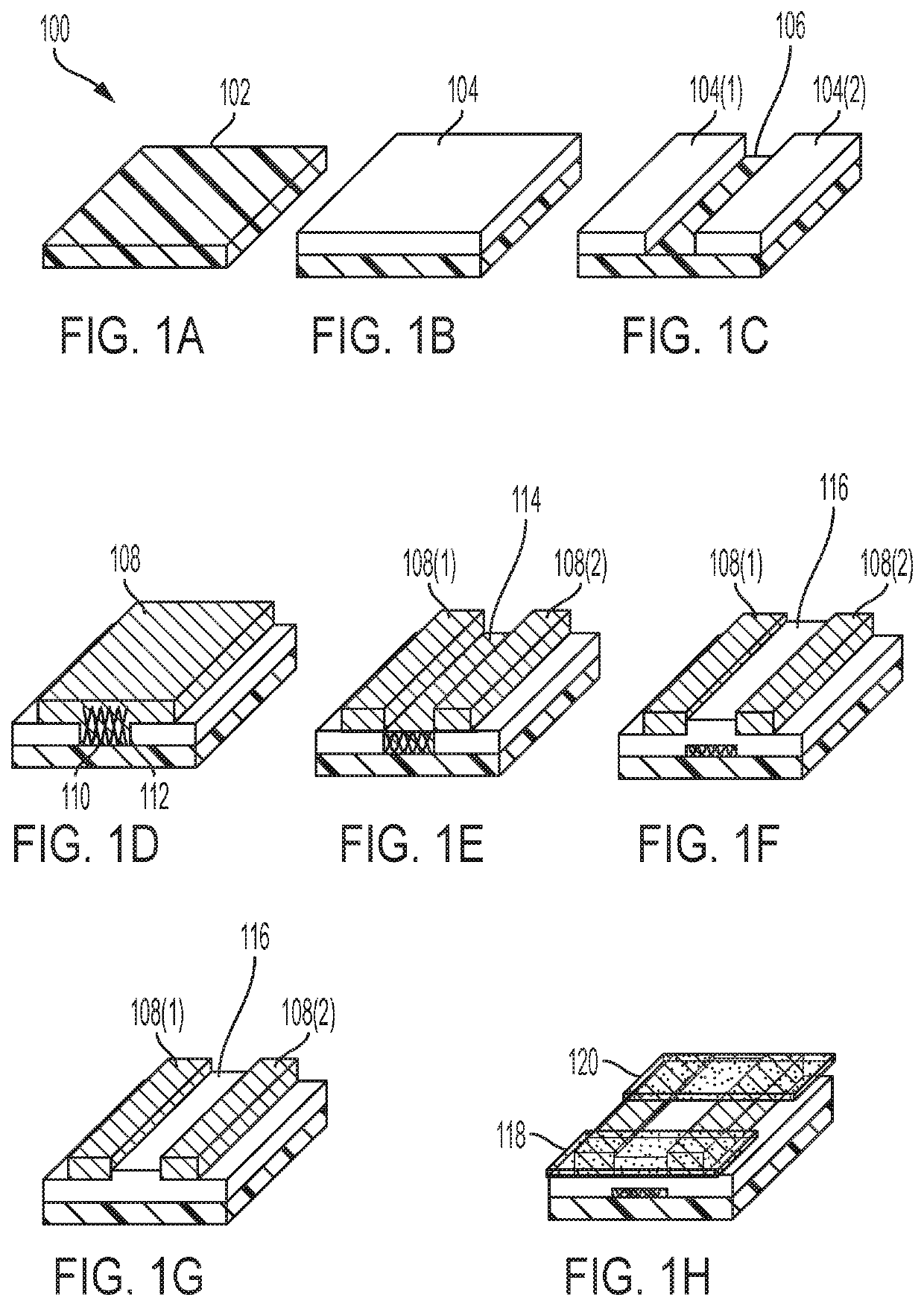
[0010]Embodiment(s) of the disclosure will now be described more fully with reference to the accompanying Drawings. The disclosure may, however, be embodied in many different forms and should not be construed as limited to the embodiment(s) set forth herein. The disclosure should only be considered limited by the claims as they now exist and the equivalents thereof.

[0011]Disclosed is a process of making a semiconductor with improved performance and improved reliability. In exemplary embodiments, the process includes selective deposition and etching of a semiconducting material to make a semiconductor with significantly fewer defects, resulting in electronic devices with improved performance and reliability.

[0012]Gallium nitride (GaN) is a semiconducting material that is used in high power or high frequency electronic applications. However, to date, a cost effective native substrate does not exist. Therefore, all GaN materials and subsequent devices are grown on non-native substrates...


PUM

PropertyMeasurementUnit
widthaaaaaaaaaa
defectaaaaaaaaaa
dielectricaaaaaaaaaa

Abstract

A method of making a semiconductor device includes depositing an amorphous layer on a substrate, masking a portion of the amorphous layer, removing a portion of the amorphous layer to form a first channel into the amorphous layer, depositing a semiconductor layer onto the substrate layer, and removing at least a portion of a defect region of the semiconductor layer to form a second channel.

Description

CROSS-REFERENCES TO RELATED APPLICATIONS[0001]This application claims the benefit of priority to and incorporates by reference the entire disclosure of U.S. Provisional Patent Application No. 62 / 634,677 filed on Feb. 23, 2018.BACKGROUNDTechnical Field[0002]The present disclosure relates generally to the manufacture of improved power electronics devices (i.e., decreased defects to enhance device performance). For example, and not by way of limitation, the present disclosure relates to fabrication of semiconductors using selective area epitaxy (SAE).History of Related Art[0003]Deposition (epitaxial growth) of a semiconductor material on a foreign substrate can result in significant defect generation in the semiconductor film due to mismatch in crystal spacing and thermal properties. Defects negatively impact device performance. For example, defects can cause current leakage, lower the breakdown voltage, and change the behavior of the device in the on-state due to electrons becoming tr...

Claims


Application Information

Patent Timeline
Patent Type & Authority Patents(United States)
IPC IPC(8): H01L21/02H01L29/66
CPCH01L29/66757H01L21/02488H01L21/02532C30B25/04
Inventor BABB, MICHAEL EVERETTHARRIS, HARLAN RUSTY
Owner TEXAS A&M UNIVERSITY
Why Eureka
Try Eureka