Semiconductor device and method for fabricating the same

a technology of semiconductors and semiconductor films, applied in semiconductor devices, transistors, electrical equipment, etc., can solve the problems of increasing the leakage current flowing through the tunnel oxide film, the failure of the tunnel oxide film to be fully functional, so as to reduce the contact resistance, the charge loss of the ono film can be restrained, and the charge loss can be restrained

Inactive Publication Date: 2006-12-14
CYPRESS SEMICON CORP
View PDF9 Cites 11 Cited by
  • Summary
  • Abstract
  • Description
  • Claims
  • Application Information

AI Technical Summary

Benefits of technology

[0009] The present invention has an object to provide a highly reliable semiconductor device in which lost of charge from the ONO film can be suppressed and a method of fabricating such a semiconductor device.
[0010] According to an aspect of the present invention, there is provided semiconductor device including: a bit line formed in a semiconductor substrate; a first interconnection line provided above the bit line and connected to the bit line; and a second interconnection line provided above the first interconnection line and connected to the first interconnection line and a transistor in a peripheral region, wherein the first interconnection line is connected to the transistor through the second interconnection line only. The first interconnection line is not connected directly to the transistor in the peripheral region but is connected thereto via the second interconnection line. It is thus possible to restrain the ONO film 12 from being damaged due to charge up caused at the time of forming the interconnection lines and to improve the reliability of the semiconductor device.
[0011] The first interconnection line may be formed in the core region or a region between the core region and the peripheral region only. It is thus possible to more reliably restrain the ONO film from being damaged and to suppress charge loss from the ONO film.

Problems solved by technology

As miniaturization of memories for achievement of a higher memory density progresses, it becomes more difficult to efficiently design the floating gate type flash memories.
However, the thinning of the tunnel oxide film increases leakage current flowing through the tunnel oxide film.
Further, the tunnel oxide film becomes more defective, which may lose charge stored in the floating gate.
Thus, the floating gate type flash memories are less reliable.
However, further miniaturization of memory cells may cause charge stored in the trap layer in the ONO film to be lost.
If part of the charge is lost from the ONO film, data stored will be lost.
This causes a serious problem about the reliability of flash memories.

Method used


Image

  • Semiconductor device and method for fabricating the same
  • Semiconductor device and method for fabricating the same
  • Semiconductor device and method for fabricating the same

Examples


first embodiment

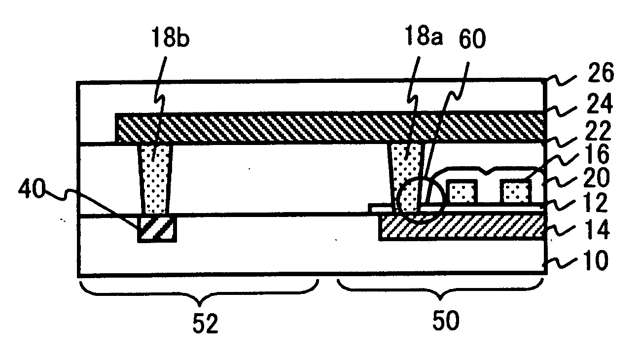
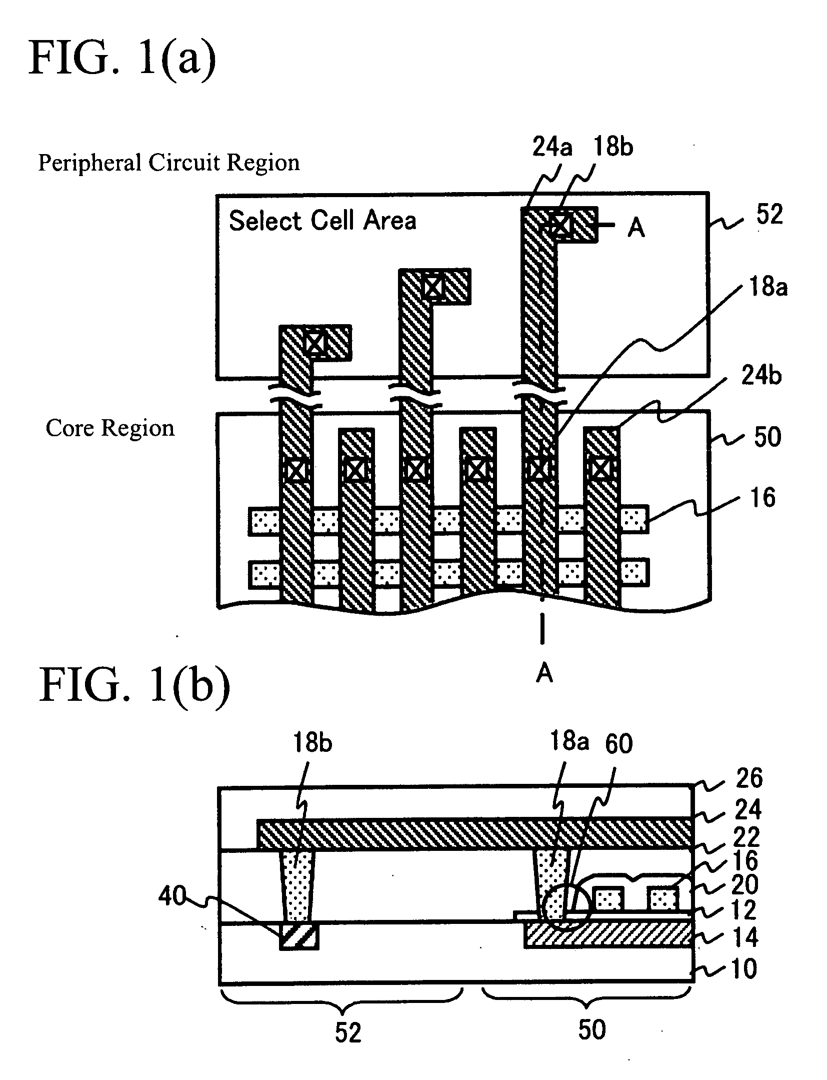
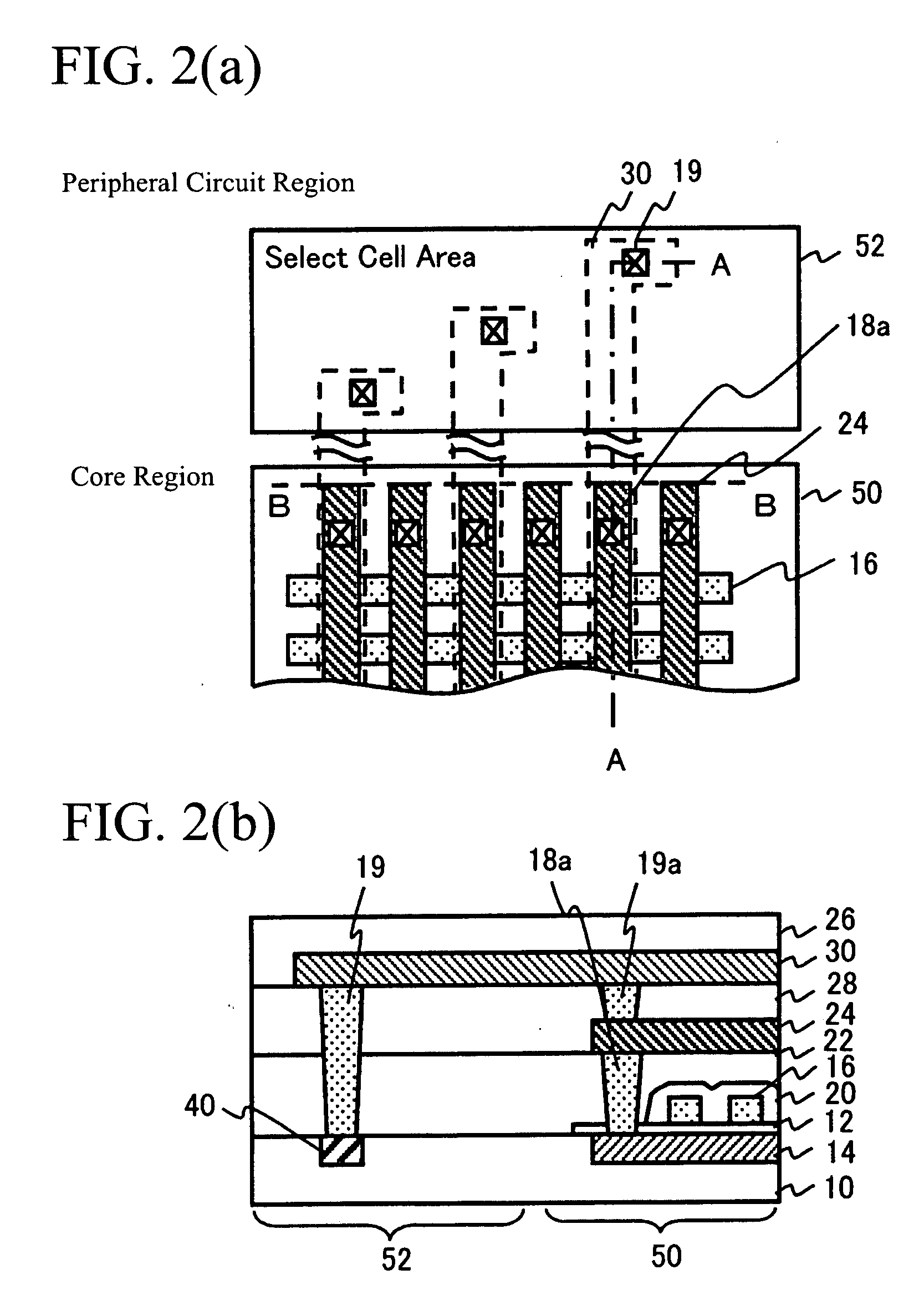
[0039] A first embodiment does not use the first interconnection lines for making connections between the transistors in the peripheral circuit region and the bit lines, but employs second interconnection lines provided on the first interconnection lines. FIG. 2(a) is a plan view of the first embodiment (in which the passivation film 26 and the interlayer insulating films 22 and 28 are not illustrated, and second interconnection lines 30 are illustrated by broken lines). FIG. 2(b) is a cross-sectional view taken along line a line A-A shown in FIG. 2(a). FIGS. 3(a) through 3(d) illustrate a method of fabricating the first embodiment, and show cross-sections corresponding to the cross section shown in FIG. 2(b). First, the fabrication method of the first embodiment is described.

[0040] Referring to FIG. 3(a), the ONO film 12 is formed on the p-type silicon semiconductor substrate 10 (or a p-type region in the semiconductor substrate 10). The ONO film 12 may be formed by forming the tu...

second embodiment

[0051] A second embodiment employs third interconnection lines 32 provided between the second interconnection lines 30 and the diffused regions 40. FIG. 4(a) is a top view of the second embodiment (in which the passivation film 26, and the interlayer insulating films 22 and 28 are not illustrated, and the second interconnection lines 30 are illustrated by broken lines). FIG. 4(b) show is a cross-sectional view taken along a line A-A shown in FIG. 4(a). FIGS. 5(a) and 5(b) show a method of fabricating the second embodiment, and illustrates cross sections taken along the line A-A. First, the fabrication method is described.

[0052] Referring to FIG. 5(a), the processes that are carried out until the first interlayer insulating film 22 is formed are the same as those shown in FIGS. 3(a) and 3(b). Contact holes 18a and 18b are formed in the first interlayer insulating film 22 so as to be connected to the bit lines 14 and the diffused regions 40. The first interconnection lines 24 that ar...

third embodiment

[0056] A third embodiment employs dummy contact holes 44 provided between the transistors in the peripheral circuit region 52 provided at each side of the core region 50 and the bit lines 14. FIG. 6(a) is a plan view (in which the passivation film 26 and the interlayer insulating film 22 are not shown), and FIG. 6(b) is a cross-sectional view taken along a line A-A shown in FIG. 6(a). FIGS. 7(a) and (b) show a method of fabricating the third embodiment, and illustrate the cross sections taken along the line A-A shown in FIG. 6(a). First, the fabrication method of the third embodiment is described.

[0057] Referring to FIG. 7(a), the ONO film 12 is formed on the p-type silicon semiconductor substrate 10 as in the case of the first embodiment. Arsenic is implanted in a given region in the semiconductor substrate in the core region 50 so as to form the bit lines 14, which function as the source and drain regions buried in the semiconductor substrate 10. Simultaneously, the dummy diffuse...


PUM


Abstract

A semiconductor device includes a bit line formed in a semiconductor substrate, a first interconnection line provided above the bit line and connected to the bit line, and a second interconnection line provided above the first interconnection line and connected to the first interconnection line and a transistor in a peripheral region. The first interconnection line is connected to the transistor through the second interconnection line only.

Description

CROSS-REFERENCE TO RELATED APPLICATIONS [0001] This is a continuation of International Application No. PCT / JP2005 / 009879 filed May 30, 2005 which was not published in English under PCT Article 21(2).BACKGROUND OF THE INVENTION [0002] 1. Field of the Invention [0003] The present invention relates to semiconductor devices and methods for the same, and more particularly, to a semiconductor device having an ONO film and its fabrication method. [0004] 2. Description of the Related Art [0005] Recently, non-volatile memories that are programmable semiconductor devices have been widely used. In the past, floating gate type flash memories were widely employed in which charge is stored in the floating gate. As miniaturization of memories for achievement of a higher memory density progresses, it becomes more difficult to efficiently design the floating gate type flash memories. The miniaturization of memory cells of the floating gate type needs thinning of the tunnel oxide film. However, the t...

Claims


Application Information

Patent Timeline
Patent Type & Authority Applications(United States)
IPC IPC(8): H01L29/788
CPCH01L27/0203H01L27/11573H01L27/11568H01L27/105H10B43/40H10B43/30H10B12/488H10B12/482
Inventor INOUE, YOKO
Owner CYPRESS SEMICON CORP
Why Eureka
Try Eureka