
Polishing pad and method of producing the same

a technology of polishing pad and polishing surface, which is applied in the field of polishing pad, can solve the problems of poor planarizing characteristics in minute regions, unpractical prior art pads, and poor polishing rate, and achieves the effects of less resistance, high polishing rate and not causing wafer breakag

Inactive Publication Date: 2006-12-14
ROHM & HAAS ELECTRONICS MATERIALS CMP HLDG INC
View PDF5 Cites 60 Cited by
  • Summary
  • Abstract
  • Description
  • Claims
  • Application Information

AI Technical Summary

Benefits of technology

[0057] When the average diameter of closed cells in the polishing layer is less than 30 μm or higher than 60 μm, the polishing rate is lowered.
[0145] The degree of swelling of the cushion layer with water is made 40% or less thereby providing a polishing pad with less reduction in hardness, less change in compressibility, thus less change in the characteristics of the whole polishing pad, and preventing the reduction in wafer yield caused by a change with time of polishing characteristics such as uniformity and polishing rate. In addition, a polishing pad with long life and a stable and high polishing rate can be obtained.

Problems solved by technology

However, the polishing pads described above suffer from the following problems:
(a) For the uniformity of whole surface, the elastic polyurethane layer in the polishing pad described in U.S. Pat. No. 3,504,457 plays a role in making loading applied to a wafer uniform, and soft synthetic leather is used in the outermost polishing layer, and therefore there is no problem such as scratches, but there is the problem of poor planarizing characteristics in minute regions.
Further, the polishing layer has a rigid foamed polyurethane layer and is thus superior to the synthetic leather in planarizing characteristics, but does not reach levels required in recent years for improving planarizing characteristics in minute regions and for polishing metal films.
The planarizing characteristics can be improved by further increasing the hardness of the rigid urethane layer, but in this case, scratches occur frequently, thus making this prior art pad unpractical.
(d) The basic idea in the polishing pad described in JP-A 10-156724 is the same as in the art described in JP-A 6-77185, and the range of the elastic modulus of each layer is limited to achieve a more efficient range, but in this art, there is no description of any substantial realizing means, thus making production of the polishing pad difficult.
However, the step for dividing the layer costs much, thus failing to provide an inexpensive polishing pad.
In the case of the polishing pads described in these prior art literatures, the polishing pads are generally stuck via an adhesive such as a double-coated tape on a polishing machine used, but their adhesiveness in this case is scarcely examined up to now.
In the case of the polishing pad used generally and widely at present, the removal of the polishing pad from a polishing machine after use requires very large force, and the exchange of the polishing pad with a new one requires severe hard work.
When the polishing pad is poor in dimensional stability, a change in dimension of the polishing pad occurs due to frictional heat generated in a polishing process, which can cause deterioration in planarizing characteristics.
Conventionally, a polishing pad is often rendered highly elastic for the purpose of improving the planarity of a material to be polished, and there is no sufficient discussion on the dimensional stability of the polishing pad.
However, when the conventional polyurethane foam sheet is used as a polishing pad or a polishing layer of a polishing pad, the polishing efficiency is improved by increasing the polishing rate, but after polishing, resistance upon removal of a wafer from the polishing pad is increased to generate dechucking error to cause problems of wafer breakage and reduction of operational efficiency.
However, when the polishing rate of the polishing pad during use is changed, it is necessary to regulate the polishing conditions, resulting in low polishing efficiency.
However, when fine particles or hollow fine particles of water-soluble resin, or polystyrene foamed beads, are dispersed in resin in the known polishing pads described above, uneven dispersion of the particles occur readily due to e.g. a difference in density from the polyurethane as matrix resin.
On the other hand, when a polishing pad consisting of foamed polyurethane obtained by reacting and curing an isocyanate group-containing compound with an active hydrogen group-containing compound is used, sufficient polishing performance may not be obtained even if the same components are used, and thus there is demand for improvement.
This increase in temperature changes the hardness (modulus of elasticity) of the polishing pad, thus exerting adverse influence on planarizing processing requiring a high degree of surface planarity.
However, it cannot be said that the planarity of this polishing pad comprising high-pressure-gas-containing hollow fine spheres dispersed therein is sufficiently satisfactory.
However, when such a hard pad is used, there occurs a problem of scratches on the polished surface of a workpiece, as described in the above literature (ibid.).
Further, the polishing pad in a non-foam system cannot sufficiently maintain slurry abrasive grains on the surface of the pad at the time of polishing, and is thus not preferable from the viewpoint of polishing rate.
However, the characteristics of this polishing pad depend greatly on the water-soluble material, and scratches caused by the thermoplastic polymer as a major component of the polishing pad cannot be solved.
When the polishing pad is poor in wetting properties with polishing slurry, the polishing slurry cannot sufficiently spread on the polishing pad, and in an extreme case, the polishing pad repels the polishing slurry to reduce the polishing rate significantly thus necessitating a long time for polishing.
Even if the polishing slurry spreads on the polishing pad, the amount of the adhering polishing slurry is uneven, thus failing to uniformly polish an object of polishing.
Further, dry regions may occur on the polishing pad, and when a small amount of polishing slurry adheres to such regions, the solution only is removed by evaporation etc., resulting in aggregation of abrasive grains on the regions, which can cause scratches as defects on the surface of a semiconductor wafer.
On the other hand, when the polishing pad is too excellent in wetting properties with polishing slurry, the solution in the polishing slurry is absorbed into the surface of the polishing pad, resulting in swelling of the polishing pad to deteriorate the stability of polishing rate.
For the purpose of improving the planarity of an object of polishing, the polishing pad is often rendered highly elastic, and there was no sufficient discussion on the wetting properties of the polishing pad.
Accordingly, chemicals for hydrophilization treatment are necessary in producing the polishing pad, and the step of hydrophilization treatment is also necessary, thus hardly coping with demand for reduction in costs.
However, the polyurethane foamed sheet is excellent in topical planarizing performance, but is poor in cushioning properties due to a low compressibility of about 0.5 to 1.0%, thus hardly giving uniform pressure on the whole surface of a wafer.
As a result, the hardness, compressibility etc. of the cushion layer are changed, the characteristics of the whole polishing pad are changed, and polishing characteristics such as uniformity and polishing rate are changed with time to cause a problem of a reduction in wafer yield.
In the technique described in Japanese Patent No. 2842865, however, the polishing layer should be in a such special shape as to cover a side of a cushion layer, and the backside of the polishing layer should form a concave so as to embed and laminate the cushion layer therein, thus significantly reducing the productivity of the polishing pad.
In the technique disclosed in Japanese Patent No. 3152188, a waterproof material layer is arranged between polishing layers, and when the polishing surface approaches the waterproof material layer as the polishing layer is abraded during polishing, the difference in rigidity between the polishing layer and waterproof material layer comes to be significant, to exert adverse influence on the polishing characteristics.

Method used


Image

  • Polishing pad and method of producing the same
  • Polishing pad and method of producing the same
  • Polishing pad and method of producing the same

Examples


examples 1 to 3

[0237]

[0238] (Evaluation of Polishing Characteristics)

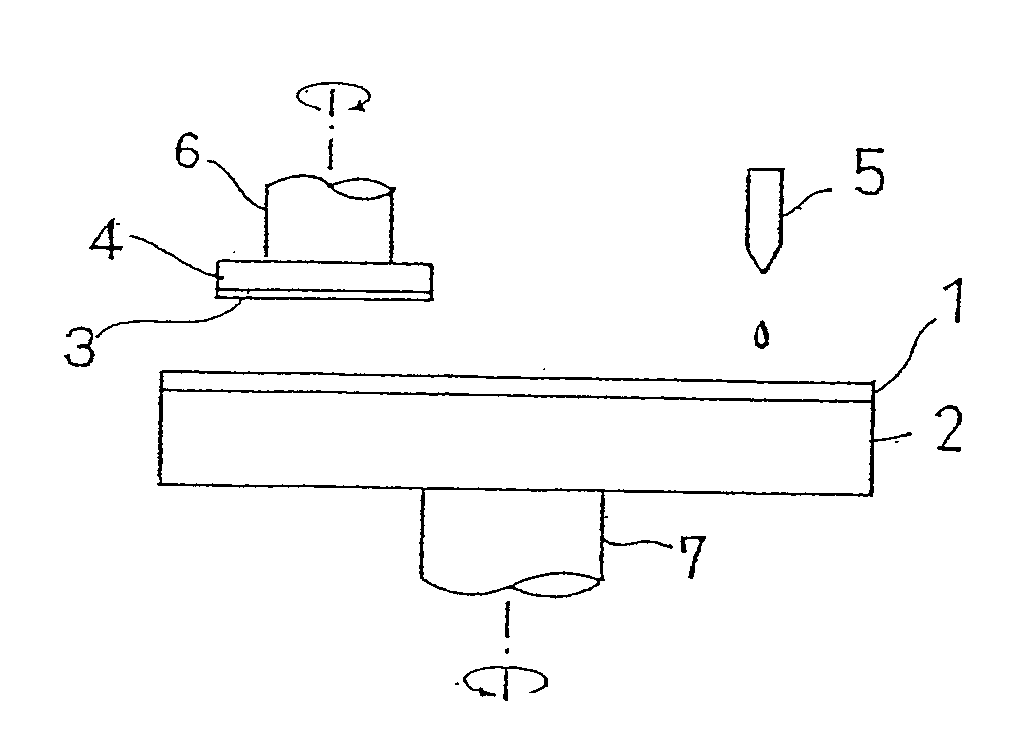
[0239] As the polishing apparatus, SPP600S manufactured by Okamoto Machine Tool Works, Ltd. was used in evaluation of polishing characteristics. The thickness of an oxide film was measured by an interference film thickness measuring device manufactured by Otsuka Denshisha. The polishing conditions were as follows: slurry SemiSperse-12 (manufactured by Cabot) was dropped at a flow rate of 150 ml / min., the polishing loading was 350 g / cm2, the number of revolutions of the polishing platen was 35 rpm, and the number of revolutions of the wafer was 30 rpm.

[0240] For evaluation of polishing characteristics, a 0.5 μm thermal-oxide film was deposited on an 8-inch silicone wafer and subjected to the following patterning (270 / 30 and 30 / 270 line / space), and then a 1 μm oxide film of p-TEOS was deposited thereon, to prepare a wafer having a pattern with an initial difference in level of 0.5 μm. This wafer was polished under the above-descr...

example 1

Example 1-1

[0256] parts by weight of a polyether-based urethane prepolymer (Adiprene L-325 manufactured by Uniroyal) and 120 parts by weight of a silicone-based surfactant SH192 (dimethyl polysiloxane / polyoxyalkylene glycol copolymer manufactured by Toray Dow Corning Silicone Co., Ltd.) were introduced into a vessel and mixed at about 900 rpm with a stirrer to produce a foamed solution (cell dispersion), and thereafter, the stirrer was exchanged with another stirrer, and 770 parts by weight of molten 4,4′-methylene-bis(2-chloroaniline) were introduced as a curing agent into it under stirring. The mixture was stirred for about 1 minute, and the mixed solution was introduced into a pan-type open mold and post-cured for 6 hours in an oven at 1110° C., to produce a foamed polyurethane block. The resulting foamed polyurethane had 350 cells / mm2, an Asker D hardness of 52, a compressibility of 2.0%, a storage elastic modulus of 279 MPa, a specific gravity of 0.8 and an average cell diamet...

example 1-2

[0259] A polishing pad was prepared in the same manner as in Example 1 except that the amount of the silicone-based surfactant SH-192 in Example 1-1 was changed to 50 parts by weight. The resulting foamed polyurethane had 230 cells / mm2, a D hardness of 58, a compressibility of 1.4%, a storage elastic modulus of 295 MPa, a specific gravity of 0.87 and an average cell diameter of 35 μm. By elementary analysis with fluorescent X rays, Si was detected, and it was thus confirmed that the predetermined surfactant was contained.


PUM

PropertyMeasurementUnit
diameteraaaaaaaaaa
pHaaaaaaaaaa
storage elastic modulusaaaaaaaaaa

Abstract

The invention provides a polishing pad by which optical materials such as lenses, reflecting mirrors etc., or materials requiring a high degree of surface planarity, as in the polishing of silicone wafers, glass substrates or aluminum substrates for hard disks, or general metal polishing, can be flattened with stability and high polishing efficiency. The invention also provides a polishing pad for semiconductor wafers, which is superior in planarizing characteristic, is free from scratches and can be produced at low cost. There is provided a polishing pad which is free from dechucking error so that neither damage to wafers nor decrease in operating efficiency occurs. There is provided a polishing pad which is satisfactory in planarity, within wafer uniformity, and polishing rate and produces less change in polishing rate. There is provided a polishing pad which can make planarity improvement and scratch decrease compatible.

Description

[0001] This is a divisional application of U.S. patent application Ser. No. 10 / 494,249, filed Nov. 3, 2004, Which is the U.S. National Phase under 35 U.S.C. §371 of International Application PCT / JP2002 / 10310, filed Oct. 2, 2002, which claims priority under 35 U.S.C. § 119 to Japanese Patent Application No. 2001-347585, filed Nov. 13, 2001; No. 2001-347538, filed November 13; No. 2001; 2001-347410, filed Nov. 13, 2001; No. 2001-351629, filed Nov. 16, 2001; No. 2001-374223, filed Dec. 7, 2001; No. 2001-374354, filed Dec. 7, 2001; No. 2001-375954, filed Dec. 10, 2001; No. 2001-378181, filed Dec. 12, 2001; No. 2002-105459, filed Apr. 8, 2002; No. 2002-117767, filed Apr. 19, 2002; No. 2002-117623, filed Apr. 19, 2002; No. 2002-144617, filed May 20, 2002; No. 2002-144628, filed May 20, 2002; and No. 2002-146495, filed May 21, 2002. The International Application was not published under PCT Article 21(2) in English.BACKGROUND OF THE INVENTION [0002] 1. Field of the Invention [0003] The pres...

Claims


Application Information

Patent Timeline
Patent Type & Authority Applications(United States)
IPC IPC(8): B32B3/26B24B9/00B24B7/00B24B37/24B24D3/30C08G18/00C08G18/10C08G18/12C08G18/66C08G18/72H01L21/306
CPCB24B37/24B24D3/30H01L21/30625C09D175/08C08L83/00C08J2483/00C08J2375/04C08J2205/052C08J9/0061C08G2101/0066C08G2101/00C08G18/724C08G18/6674B24D18/00C08G18/00C08G18/10C08G18/12C08G18/4211C08G18/4236C08G18/4808C08G18/4854C08G18/61C08G18/664C08G18/3814C08G18/3243C08G18/5096Y10T428/249976Y10T428/249953C08G2110/0066H01L21/304
Inventor SHIMOMURA, TETSUONAKAMORI, MASAHIKOYAMADA, TAKATOSHIMASUI, TAKASHIKOMAI, SHIGERUONO, KOICHIOGAWA, KAZUYUKIKAZUNO, ATSUSHIKIMURA, TSUYOSHISEYANAGI, HIROSHI
Owner ROHM & HAAS ELECTRONICS MATERIALS CMP HLDG INC
Learn More