Supercharge Your Innovation With Domain-Expert AI Agents!

Shadow mask deposition of materials using reconfigurable shadow masks

a technology of shadow mask and material, applied in the field of forming electronic devices, to achieve the effect of facilitating the deposition of materials

Active Publication Date: 2006-12-14
ADVANTECH GLOBAL LTD
View PDF20 Cites 8 Cited by
  • Summary
  • Abstract
  • Description
  • Claims
  • Application Information

AI Technical Summary

Benefits of technology

[0025] The electronic element can be thin film transistor (TFT), a diode, a memory element, a capacitor, or any combination of the foregoing. The electronic device can also include interconnects formed from one or mor

Problems solved by technology

One problem with the current shadow mask deposition process is the need to engineer, manufacture and inventory a large number of shadow masks, each of which typically has one or more apertures of a unique size and / or location in the shadow mask.

Method used


Image

  • Shadow mask deposition of materials using reconfigurable shadow masks
  • Shadow mask deposition of materials using reconfigurable shadow masks
  • Shadow mask deposition of materials using reconfigurable shadow masks

Examples


Embodiment Construction

[0036] The present invention will be described with reference to the accompanying figures where like reference numbers correspond to like elements.

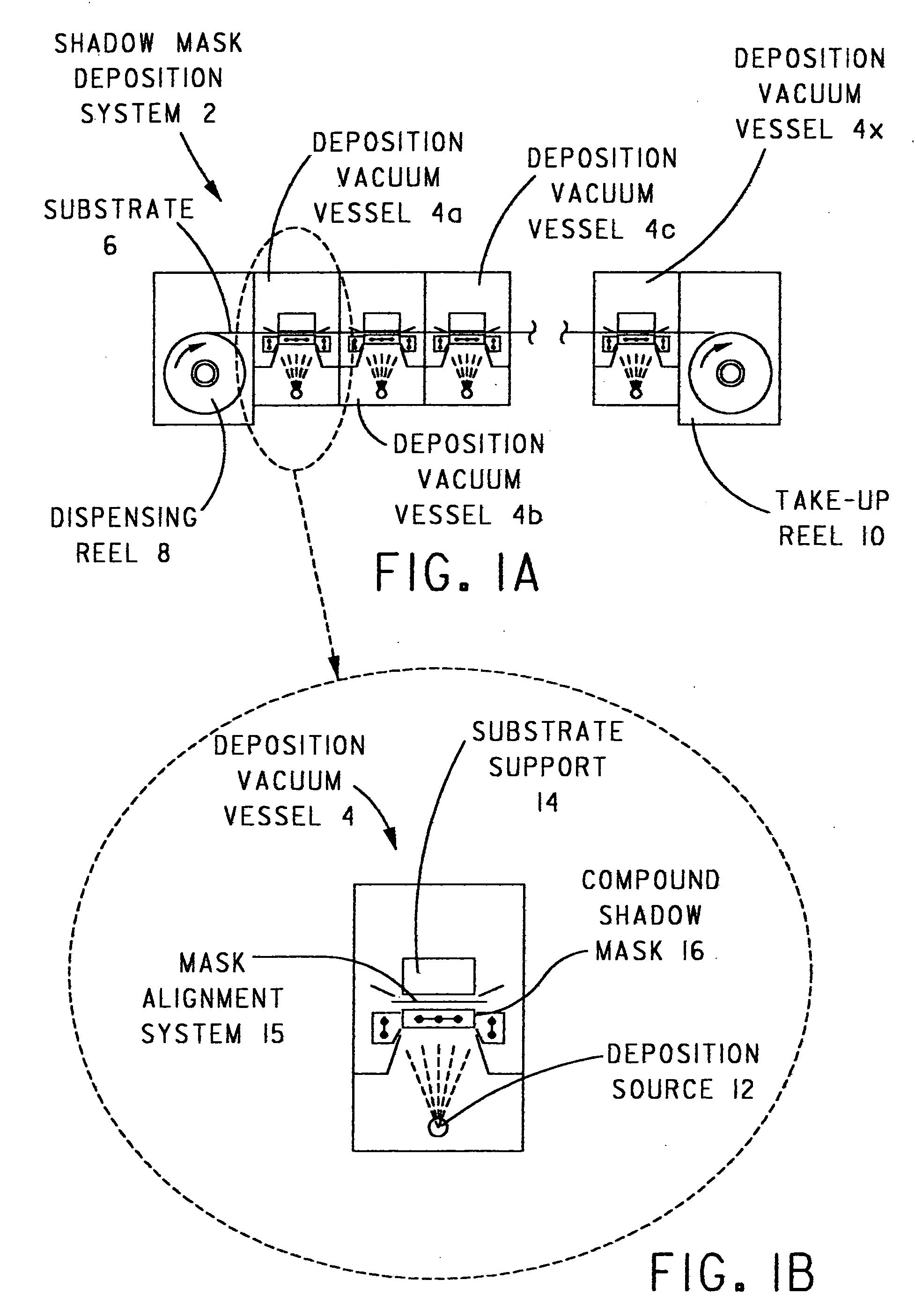
[0037] With reference to FIGS. 1A and 1B, a shadow mask deposition system 2 for forming an electronic device, such as, without limitation, a high resolution active matrix light emitting diode (LED) display, includes a plurality of serially arranged deposition vacuum vessels 4 (e.g., deposition vacuum vessels 4a-4x). The number and arrangement of deposition vacuum vessels 4 is dependent on the number of deposition events required for any given product to be formed therewith.

[0038] In use of shadow mask deposition system 2, a flexible substrate 6 translates through the serially arranged deposition vacuum vessels 4 by means of a reel-to-reel mechanism that includes a dispensing reel 8 and a take-up reel 10.

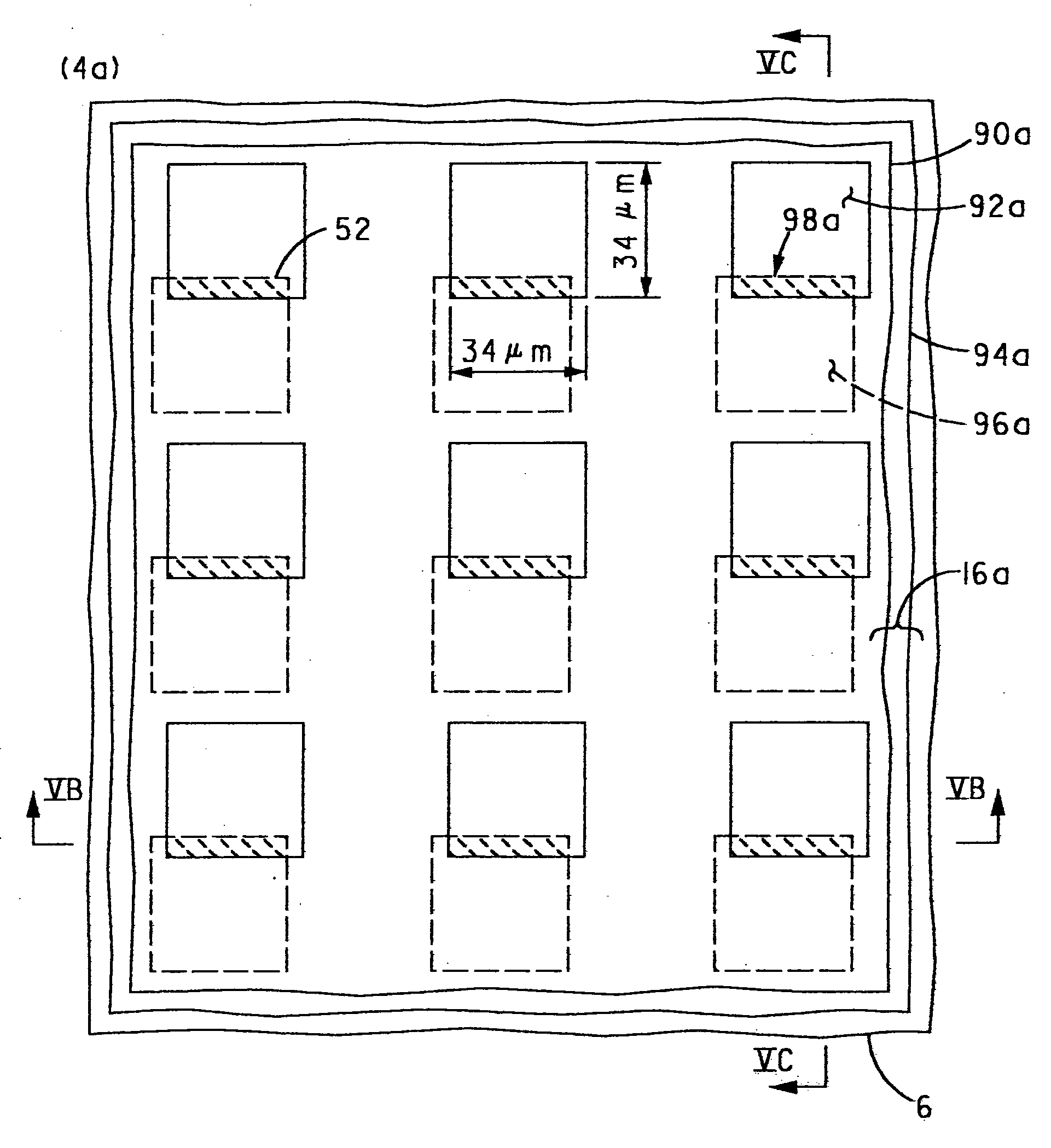
[0039] Each deposition vacuum vessel includes a deposition source 12, a substrate support 14, a mask alignment system 15 and a compoun...


PUM

PropertyMeasurementUnit
Fractionaaaaaaaaaa
Timeaaaaaaaaaa
Timeaaaaaaaaaa

Abstract

A shadow mask deposition system includes a plurality of identical shadow masks arranged in a number of stacks to form a like number of compound shadow masks, each of which is disposed in a deposition vacuum vessel along with a material deposition source. Materials from the material deposition sources are deposited on the substrate via openings in corresponding compound shadow masks, each opening being formed by the whole or partial alignment of apertures in the shadow masks forming the compound shadow mask, to form an array of electronic elements on the substrate.

Description

BACKGROUND OF THE INVENTION [0001] 1. Field of the Invention [0002] The present invention relates to a method of forming an electronic device on a substrate and, more particularly, to a method of forming one or more electronic elements of the electronic device on the substrate by way of a shadow mask deposition process. [0003] 2. Description of Related Art [0004] Electronic circuits with repetitive patterns, such as memories and imaging or display devices are, widely used in LED industry. Presently, such circuits are formed by photolithographic processes. [0005] A shadow mask deposition process is well-known and has been used for years in micro-electronics manufacturing. The shadow mask process is a significantly less costly and less complex manufacturing process compared to the photolithography process. Accordingly, it would be desirable to utilize the shadow mask deposition process to form electronic circuits. [0006] One problem with the current shadow mask deposition process is t...

Claims


Application Information

Patent Timeline
IPC IPC(8): H01L21/00
CPCC23C14/042C23C14/562Y10S438/944H01L27/14683H01L27/1214H01L27/1288
Inventor BRODY, THOMAS PETER
Owner ADVANTECH GLOBAL LTD
Features
  • R&D
  • Intellectual Property
  • Life Sciences
  • Materials
  • Tech Scout
  • Unparalleled Data Quality
  • Higher Quality Content
  • 60% Fewer Hallucinations
Learn More