Honeycomb optical window deposition shield and method for a plasma processing system

Inactive Publication Date: 2005-10-13
TOKYO ELECTRON LTD
View PDF2 Cites 14 Cited by
  • Summary
  • Abstract
  • Description
  • Claims
  • Application Information

AI Technical Summary

Benefits of technology

[0012] Still another object of the present invention is to provide an optical window deposition shield

Problems solved by technology

The erosion or coating of exposed components in the plasma processing system can lead to a gradual degradation of the plasma processing performance and ultimately to complete failure of the system.
While these high aspect ratio holes 7 allow viewing through the optical window deposition shield 1, because of their geometry, the high aspect ratio holes 7 do not allow plasma to form close to the optical window of a plasma chamber that the shield is used in.
While effective in shielding the optical window of a processing chamber, prior art optical window deposition shields such as the one shown in FIG. 6 pose problems.
First, the process of forming multiple holes in a block of aluminum does not provide a large ratio of viewi

Method used


Image

  • Honeycomb optical window deposition shield and method for a plasma processing system
  • Honeycomb optical window deposition shield and method for a plasma processing system
  • Honeycomb optical window deposition shield and method for a plasma processing system

Examples


Embodiment Construction

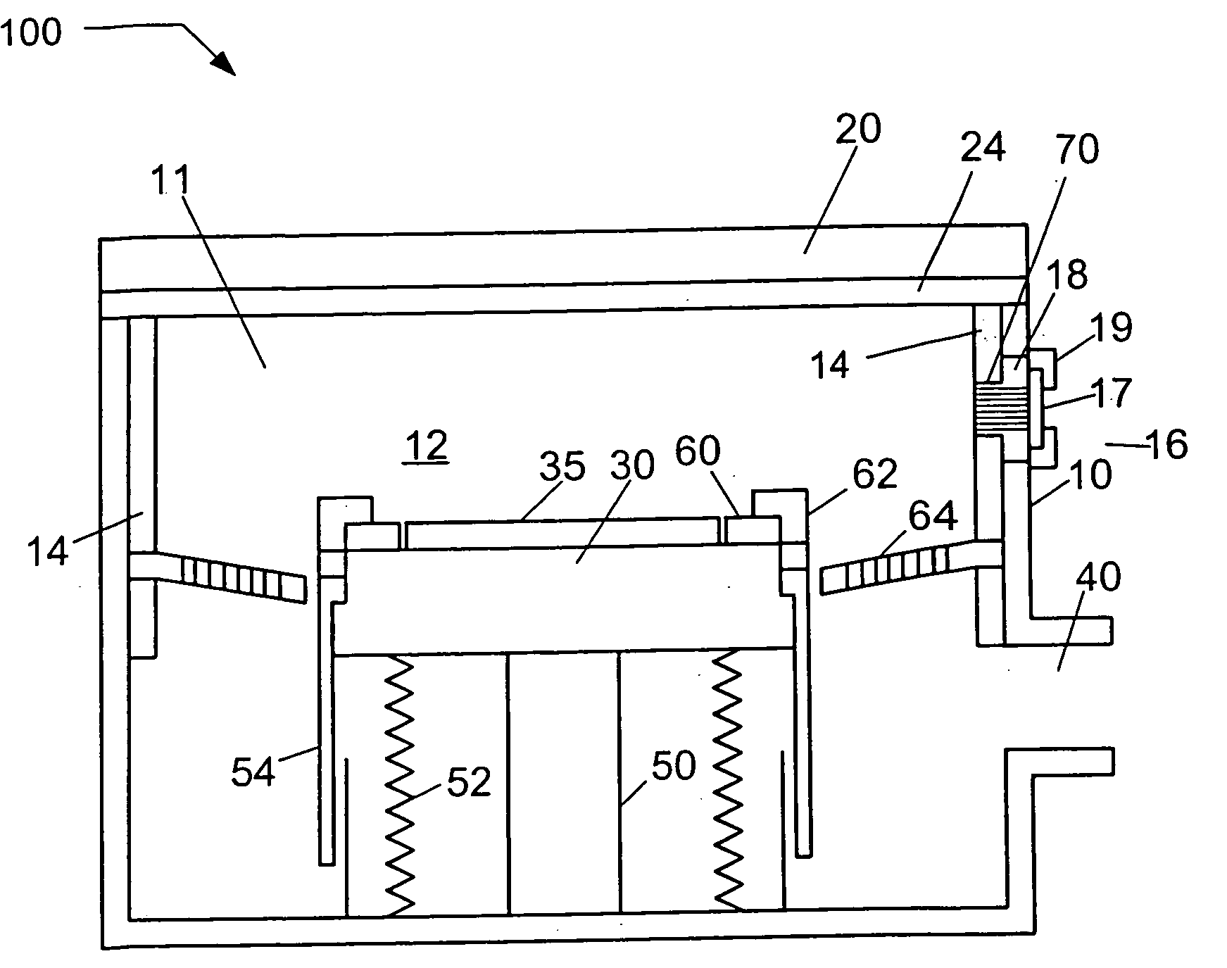
[0030] Referring now to the drawings, wherein like reference numerals designate identical or corresponding parts throughout the several views. FIG. 1 shows a simplified block diagram of a plasma processing system according to an embodiment of the present invention. As seen in this figure, a plasma processing system 100 includes a plasma processing chamber 10, an upper assembly 20, an electrode plate 24, a substrate holder 30 for supporting a substrate 35, and a pumping duct 40 coupled to a vacuum pump (not shown) for providing a reduced pressure atmosphere 11 in plasma processing chamber 10. Plasma processing chamber 10 can facilitate the formation of processing plasma in a process space 12 adjacent substrate 35. The plasma processing system 100 can be configured to process 200 mm substrates, 300 mm substrates, or larger.

[0031] In the illustrated embodiment, the upper assembly 20 can include at least one of a cover, a gas injection assembly, and an upper electrode impedance match n...


PUM

PropertyMeasurementUnit
Lengthaaaaaaaaaa
Diameteraaaaaaaaaa
Structureaaaaaaaaaa

Abstract

An optical window deposition shield including a backing plate having a through hole, and a honeycomb structure having a plurality of adjacent cells configured to allow optical viewing through the honeycomb structure. Each cell of the honeycomb structure has an aspect ratio of length to diameter sufficient to impede a processing plasma from traveling through the full length of the cell. A coupling device configured to couple the honeycomb core structure to the backing plate such that the honeycomb structure is aligned with at least a portion of the through hole in the backing plate. The optical window deposition shield shields the optical viewing window of a plasma processing apparatus from contact with the plasma.

Description

BACKGROUND OF THE INVENTION [0001] 1. Field of the Invention [0002] The present invention relates to an improved component for a plasma processing system and, more particularly, to an optical window deposition shield employed in a plasma processing system to provide optical access to a process space through the deposition shield. [0003] 2. Discussion of the Background [0004] The fabrication of integrated circuits (IC) in the semiconductor industry typically employs plasma to create and assist surface chemistry within a plasma reactor necessary to remove material from and deposit material to a substrate. In general, plasma is formed with the plasma reactor under vacuum conditions by heating electrons to energies sufficient to sustain ionizing collisions with a supplied process gas. Moreover, the heated electrons can have energy sufficient to sustain dissociative collisions and, therefore, a specific set of gasses under predetermined conditions (e.g. chamber pressure, gas flow rate et...

Claims


Application Information

Patent Timeline
IPC IPC(8): C23C14/00H01J7/24H01J17/26H01J37/32H01L21/00
CPCH01J37/32458H01J37/32972H01L21/67069
Inventor FINK, STEVEN T.MITROVIC, ANDREJ S.CALABRESE, PAULA A.
Owner TOKYO ELECTRON LTD
Why Eureka
Try Eureka