

Method for forming a sealed storage non-volative multiple-bit memory cell
a non-volatile, memory cell technology, applied in the direction of semiconductor devices, electrical devices, transistors, etc., can solve the problems of negative charge accumulation, shortening the effective length of the channel in the memory cell, and breaking down in the insulating material, so as to reduce the bird's beak effect and low bit line resistance
- Summary
- Abstract
- Description
- Claims
- Application Information
AI Technical Summary
Benefits of technology
Problems solved by technology
Method used
Image

Examples
Embodiment Construction
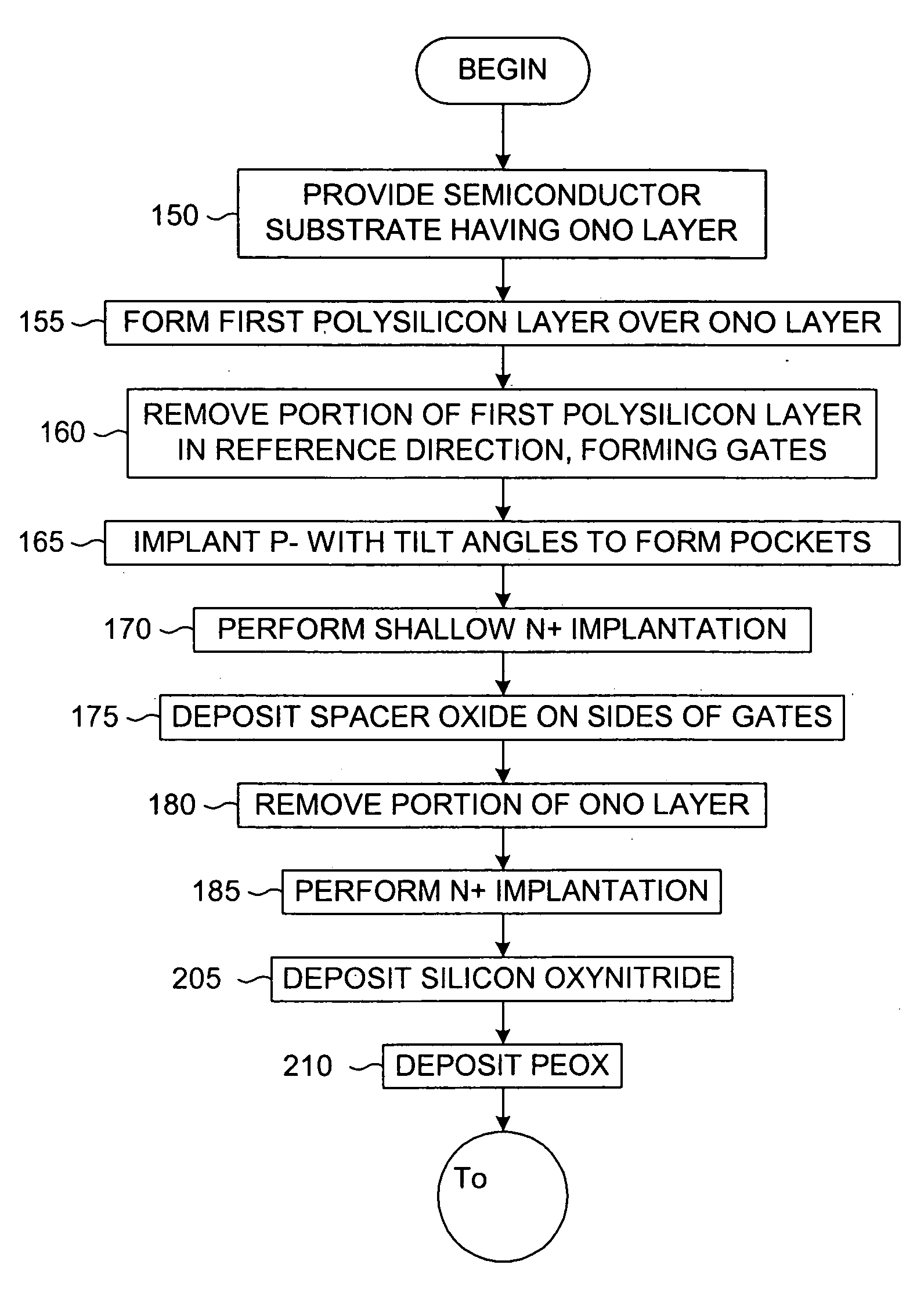
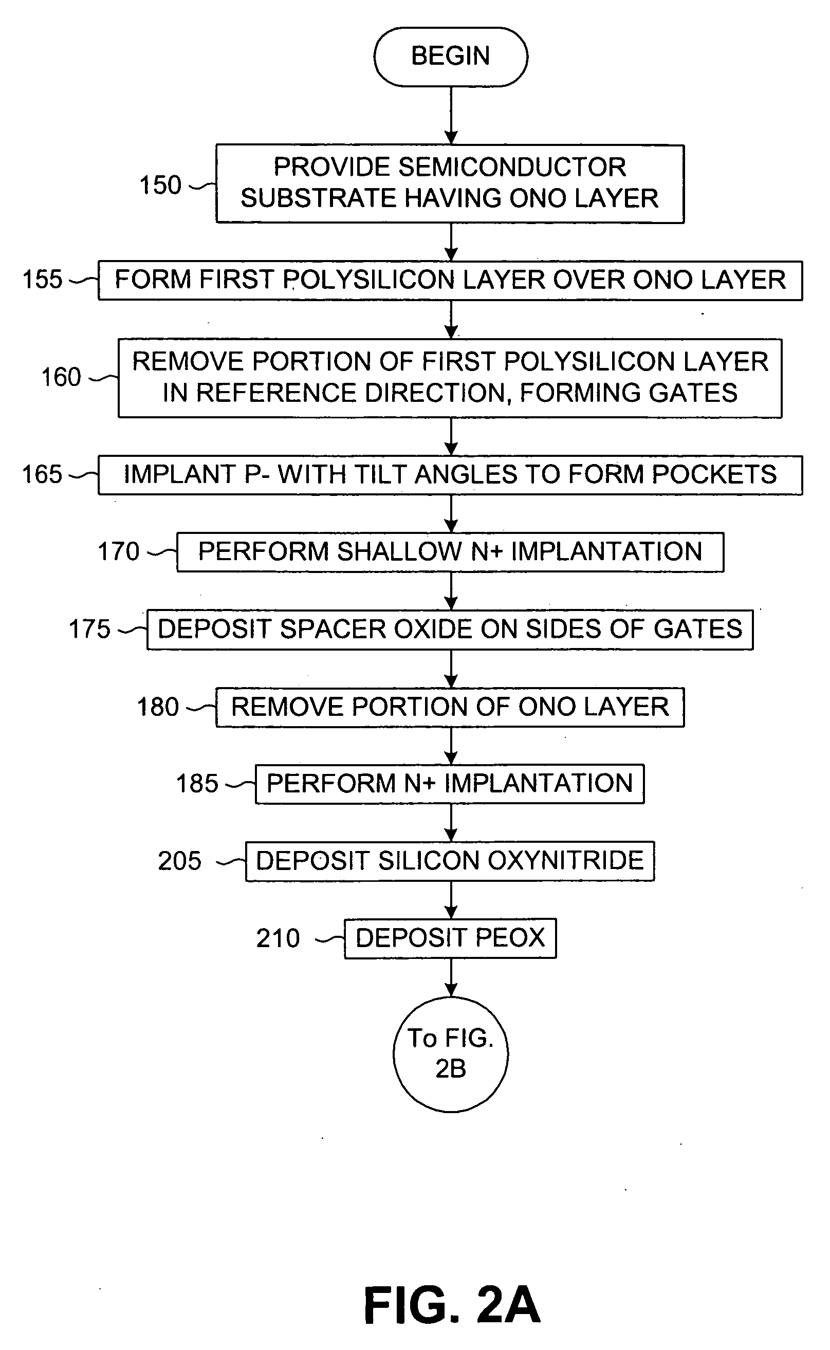
[0039] Reference will now be made in detail to the presently preferred embodiments of the invention, examples of which are illustrated in the accompanying drawings. Wherever possible, the same or similar reference numbers are used in the drawings and the description to refer to the same or like parts. It should be noted that the drawings are in simplified form and are not to precise scale. In reference to the disclosure herein, for purposes of convenience and clarity only, directional terms, such as, top, bottom, left, right, up, down, over, above, below, beneath, rear, and front, are used with respect to the accompanying drawings. Such directional terms should not be construed to limit the scope of the invention in any manner.
[0040] Although the disclosure herein refers to certain illustrated embodiments, it is to be understood that these embodiments are presented by way of example and not by way of limitation. The intent of the following detailed description, although discussing ...
PUM
 Abstract
Description
Claims
Application Information