Hetero-junction bipolar transistor and manufacturing method thereof
a bipolar transistor and heterojunction technology, applied in the direction of basic electric elements, electrical appliances, semiconductor devices, etc., to achieve the effect of high performance heterojunction, good processibility, and not increasing the resistance (ron)
- Summary
- Abstract
- Description
- Claims
- Application Information
AI Technical Summary
Benefits of technology
Problems solved by technology
Method used
Image

Examples
embodiment
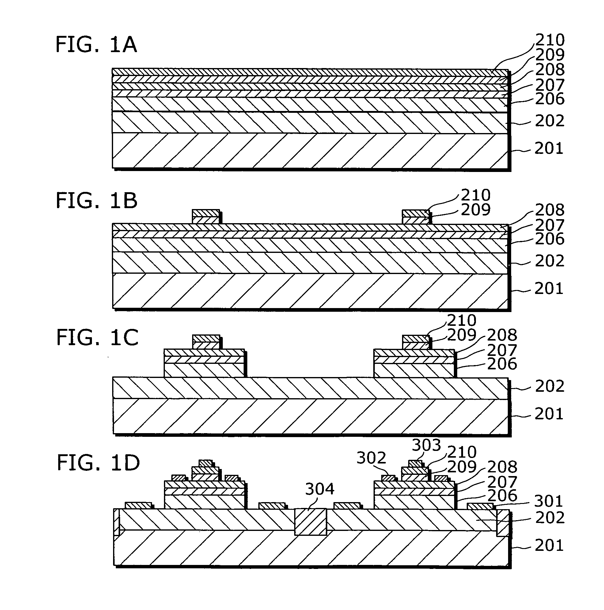
[0035] The embodiment according to the present invention is described hereinafter with reference to diagrams.
[0036] A hetero-junction bipolar transistor according to the present invention includes a collector layer made up of the following layers sequentially formed on an n-type GaAs sub-collector layer: a first collector layer made of InGaP in an ordered n-type lattice and a second collector layer made of n-type GaAs with a lower concentration than the sub-collector layer. On the second collector layer, a p-type GaAs base layer and an n-type emitter layer that is made of a semiconductor material having a larger band gap than the base layer are sequentially formed.
[0037] Considering the aforementioned structure, the hetero-junction bipolar transistor in the present embodiment is described.
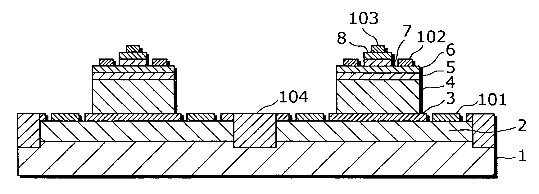
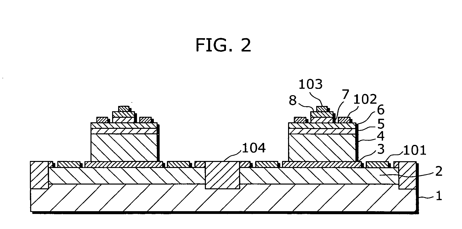
[0038]FIG. 2 is a cross-section diagram showing a structure of the hetero-junction bipolar transistor of the present invention. As shown in FIG. 2, the hetero-junction bipolar transistor (hereaf...
PUM
 Abstract
Description
Claims
Application Information
 - R&D Engineer
- R&D Manager
- IP Professional
- Industry Leading Data Capabilities
- Powerful AI technology
- Patent DNA Extraction
Browse by: Latest US Patents, China's latest patents, Technical Efficacy Thesaurus, Application Domain, Technology Topic.
© 2024 PatSnap. All rights reserved.Legal|Privacy policy|Modern Slavery Act Transparency Statement|Sitemap