Nanoelectonic devices based on nanowire networks

Inactive Publication Date: 2006-12-21
RGT UNIV OF CALIFORNIA
View PDF5 Cites 90 Cited by
  • Summary
  • Abstract
  • Description
  • Claims
  • Application Information

AI Technical Summary

Benefits of technology

[0010] In accordance with the present invention, nanoelectronic semiconductor devices are provided where networks of molecular nanowires (or nanofibers) are used in place of the conventional semiconductor materials that are present in such devices. In a particular embodiment, field effect transistors are provided where networks of molecular nanowires are used to provide the electrical connection between the sou

Problems solved by technology

However, fabrication of such devices, where a single nanowire connects the (source and drain) electrodes, are technically demanding, particularly at small dimen

Method used


Image

  • Nanoelectonic devices based on nanowire networks
  • Nanoelectonic devices based on nanowire networks
  • Nanoelectonic devices based on nanowire networks

Examples


Embodiment Construction

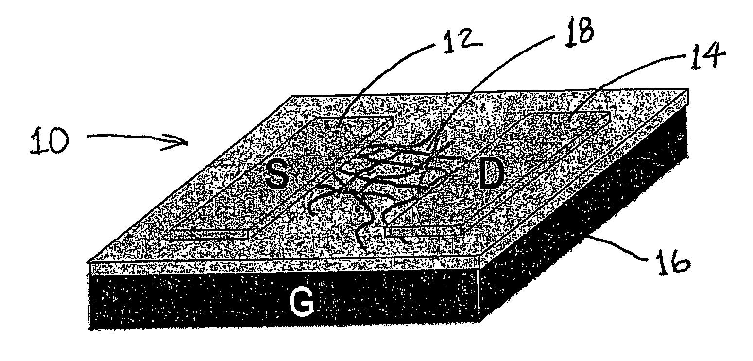
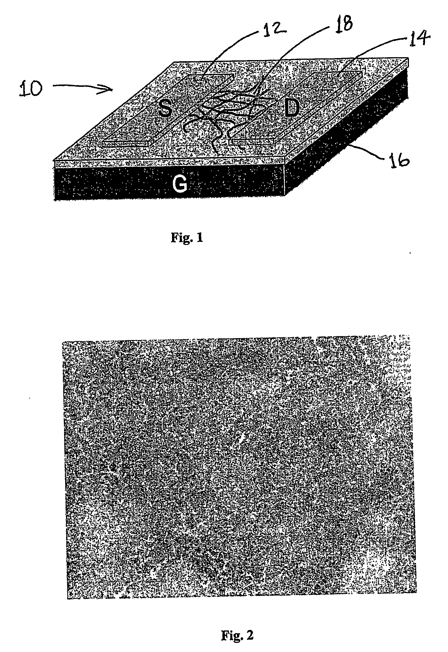
[0019] An exemplary field effect transistor (FET) that utilizes a network of molecular nanowires (or nanofibers) in accordance with the present invention is shown generally in FIG. 1 at 10. The FET 10 includes a source electrode (S) 12, a drain electrode (D) 14 and a gate electrode (G) 16. The network of molecular nanowires is shown at 18. As is typical in any FET, an electrically insulating layer 20 is provided between the gate electrode and the semiconductor material (nanowire network 18). The insulating layer can be silicon dioxide (see Ref. 202), non-conducting polymer, such as epoxy. The electrodes can be made from any of the materials used in conventional FET devices. The FET operates in the same manner as conventional FET's except that that typical semiconductor material that is present between the source and drain electrodes is replaced with a network of molecular nanowires.

[0020] For the purposes of this specification, molecular nanowires are defined as having dimensions l...


PUM


Abstract

Semiconductor devices where networks of molecular nanowires (or nanofibers) are used as the semiconductor material. Field effect transistors are disclosed where networks of molecular nanowires are used to provide the electrical connection between the source and drain electrodes. The molecular nanowires have diameters of less than 500 nm and aspect ratios of at least 10. The molecular nanowires that are used to form the networks can be single element nanowires, Group III-V nanowires, Group II-VI nanowires, metal oxide nanowires, metal chalcogenide nanowires, ternary chalcogenide nanowires and conducting polymer nanowires.

Description

BACKGROUND OF THE INVENTION [0001] 1. Field of the Invention [0002] The present invention relates generally to semiconductor devices and the materials that are used as the semiconductor elements in such devices. More particularly, the invention is directed to the use of networks of molecular nanowires as the semiconductor element in such devices. [0003] 2. Description of Related Art [0004] The publications and other reference materials referred to herein to describe the background of the invention and to provide additional detail regarding its practice are hereby incorporated by reference. For convenience, the reference materials are numerically referenced and grouped in the appended bibliography. [0005] Nanoscale electronic devices that include components other that silicon offer attractive alternatives to traditional devices made using photolithographic methods. Various wires, with dimensions less that one micron have been fabricated or grown and some of them have been demonstrate...

Claims


Application Information

Patent Timeline
IPC IPC(8): H01L29/76B82BH01L29/06H01L29/20H01L29/22H01L29/24H01L29/786H01L51/00H01L51/05
CPCB82Y10/00H01L29/0665H01L29/0673H01L29/20H01L29/22H01L51/0545H01L29/78681H01L29/7869H01L29/78696H01L51/0048H01L29/24H10K85/221H10K10/466
Inventor KANER, RICHARD B.HUANG, JIAXINGGRUNER, GEORGE
Owner RGT UNIV OF CALIFORNIA
Why Eureka
Try Eureka