

Wafer demounting method, wafer demounting device, and wafer demounting and transferring machine
a technology of wafers and transferring machines, which is applied in the direction of thin material processing, electrical equipment, article separation, etc., can solve the problems of easy accident of wafer breakage, difficulty in releasing a wafer upwards from a lower wafer adjacent thereto, etc., to achieve high convenience and increase processing efficiency
- Summary
- Abstract
- Description
- Claims
- Application Information
AI Technical Summary
Benefits of technology
Problems solved by technology
Method used
Image

Examples
Embodiment Construction
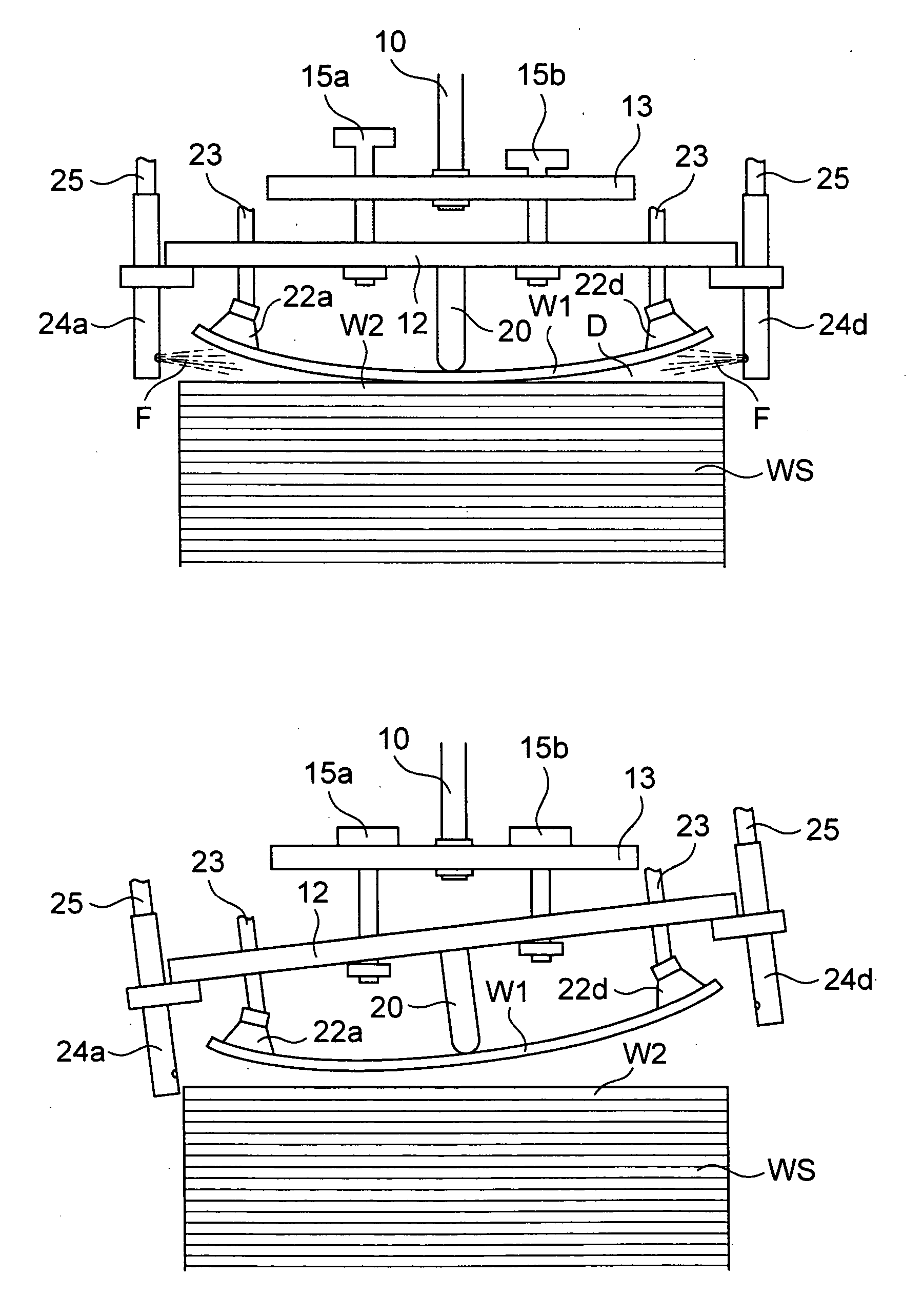
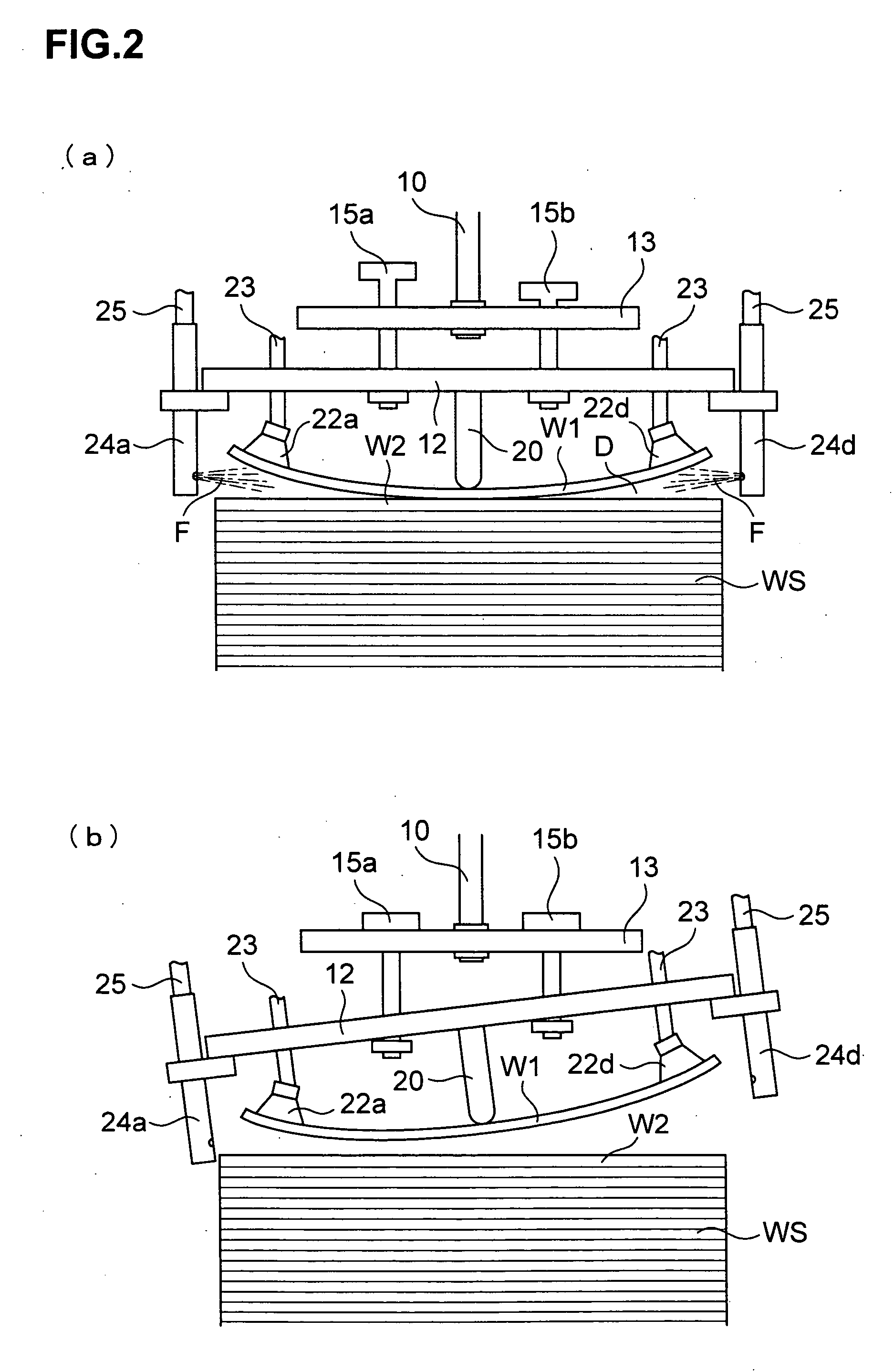
[0044] Description will be given of embodiments of the present invention below and it is needless to say that the description below is presented by way of illustration only and should not be taken by way of limitation. Incidentally, in FIGS. 1(a) and 1(b) to FIG. 10, components identical with or similar to those shown in FIG. 11 to FIGS. 12(a) and 12(b) may be denoted by the same reference symbols or similar ones.
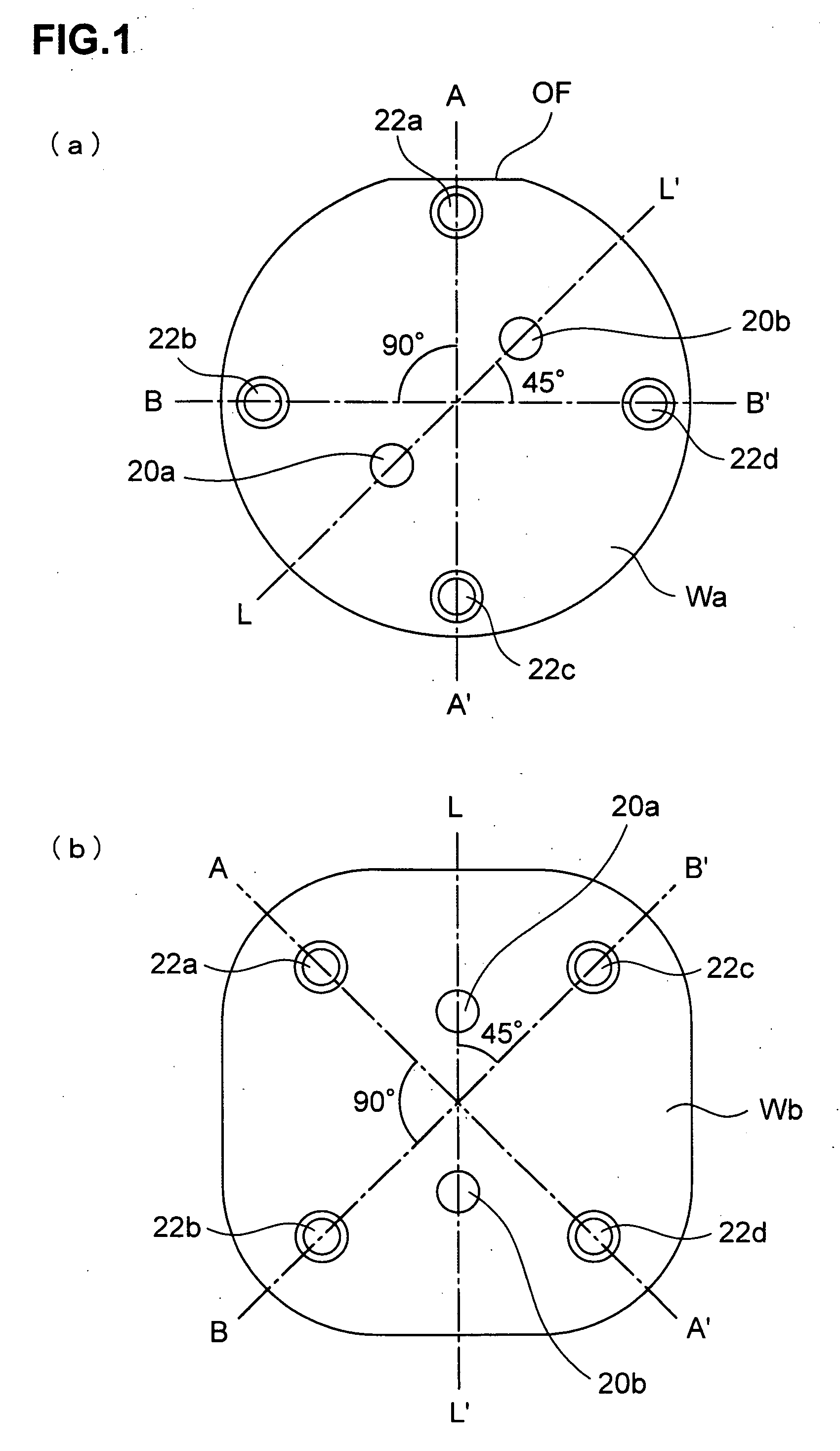
[0045] FIGS. 1(a) and 1(b) are top plan views showing vacuum chuck positions when a wafer is released by means of a wafer release method of the present invention, wherein FIG. 1(a) shows a case of a disc-like wafer, and FIG. 1(b) shows an almost tetragonal wafer.
[0046] In FIG. 1(a), a reference symbol Wa is a disk-like wafer and the wafer with a crystal orientation . A segment showing with a symbol A-A′ and a segment showing with a symbol B-B′ are crystal habit line axes and cross each other at a right angle in the central portion of the wafer. An OF (orientation flat) co...
PUM
 Abstract
Description
Claims
Application Information