Method for silicon based dielectric deposition and clean with photoexcitation

a dielectric deposition and photoexcitation technology, applied in chemical vapor deposition coating, coating, metallic material coating process, etc., can solve the problems of low film growth rate, no production worthiness suitable for large-scale semiconductor device fabrication, etc., to enhance chamber cleaning, enhance various processing attributes, and increase surface energy

Inactive Publication Date: 2006-12-21
APPLIED MATERIALS INC
View PDF19 Cites 355 Cited by
  • Summary
  • Abstract
  • Description
  • Claims
  • Application Information

AI Technical Summary

Benefits of technology

[0007] Embodiments of the invention generally provide a method for depositing films using photoexcitation. The photoexcitation may be utilized for at least one of treating the substrate prior to deposition, treating substrate and / or gases during deposition, treating a deposited film, or for enhancing chamber cleaning. The photoexcitation may be used to enhance various processing attributes, such as removing native oxides prior to deposition, removing volatiles from deposited films, increasing surface energy, increasing the excitation energy of precursors, and the like.

Problems solved by technology

Although some thermal CVD processes for silicon-containing materials having deposition temperatures less than 550 degrees Celsius have been proposed, none have exhibited production worthiness suitable for large scale utilization in semiconductor device fabrication.
While these methods have enabled a reduction in processing temperatures to about 550 degrees Celsius or less, film growth rates have been extremely low.

Method used


Image

  • Method for silicon based dielectric deposition and clean with photoexcitation
  • Method for silicon based dielectric deposition and clean with photoexcitation
  • Method for silicon based dielectric deposition and clean with photoexcitation

Examples


Embodiment Construction

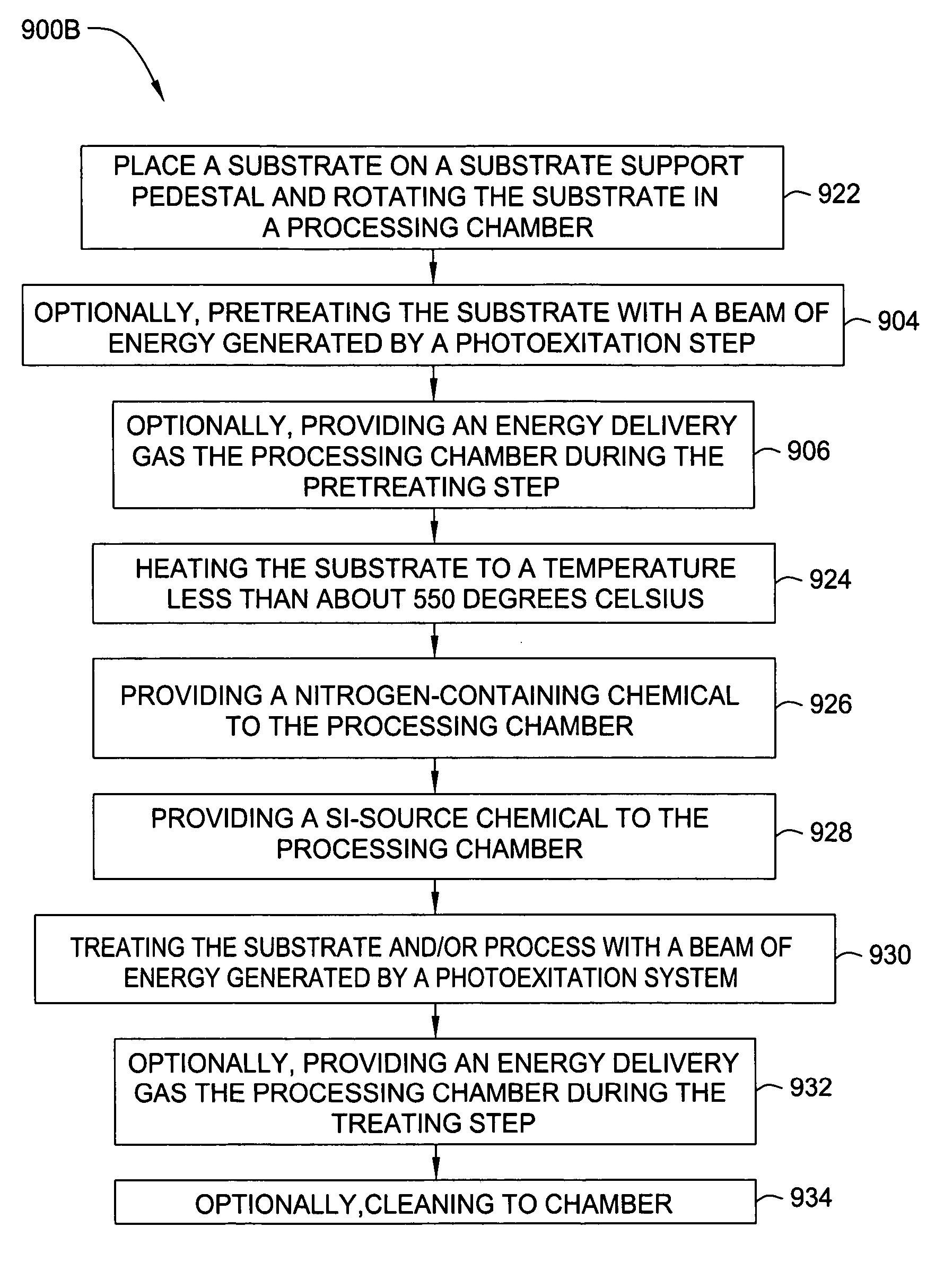
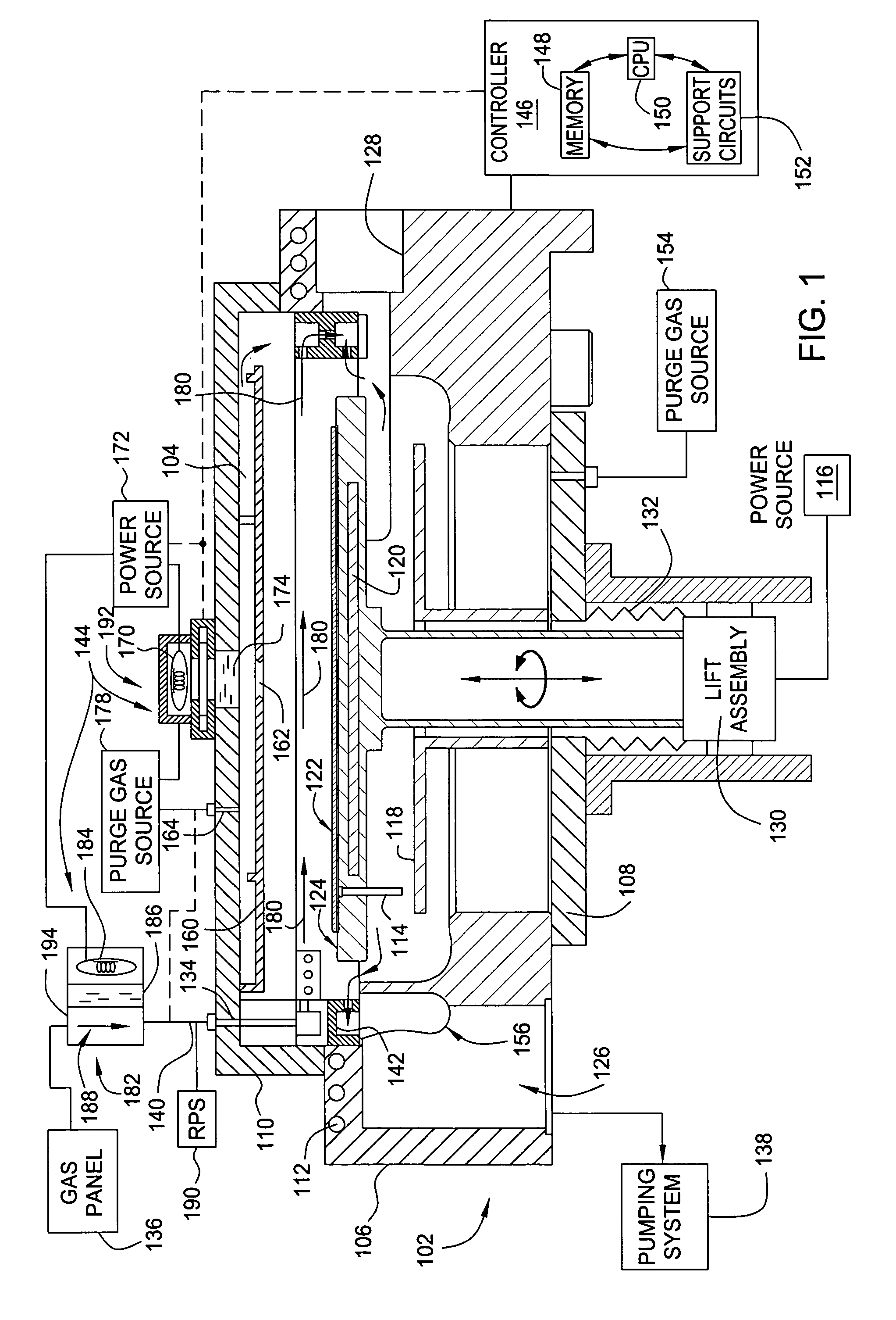
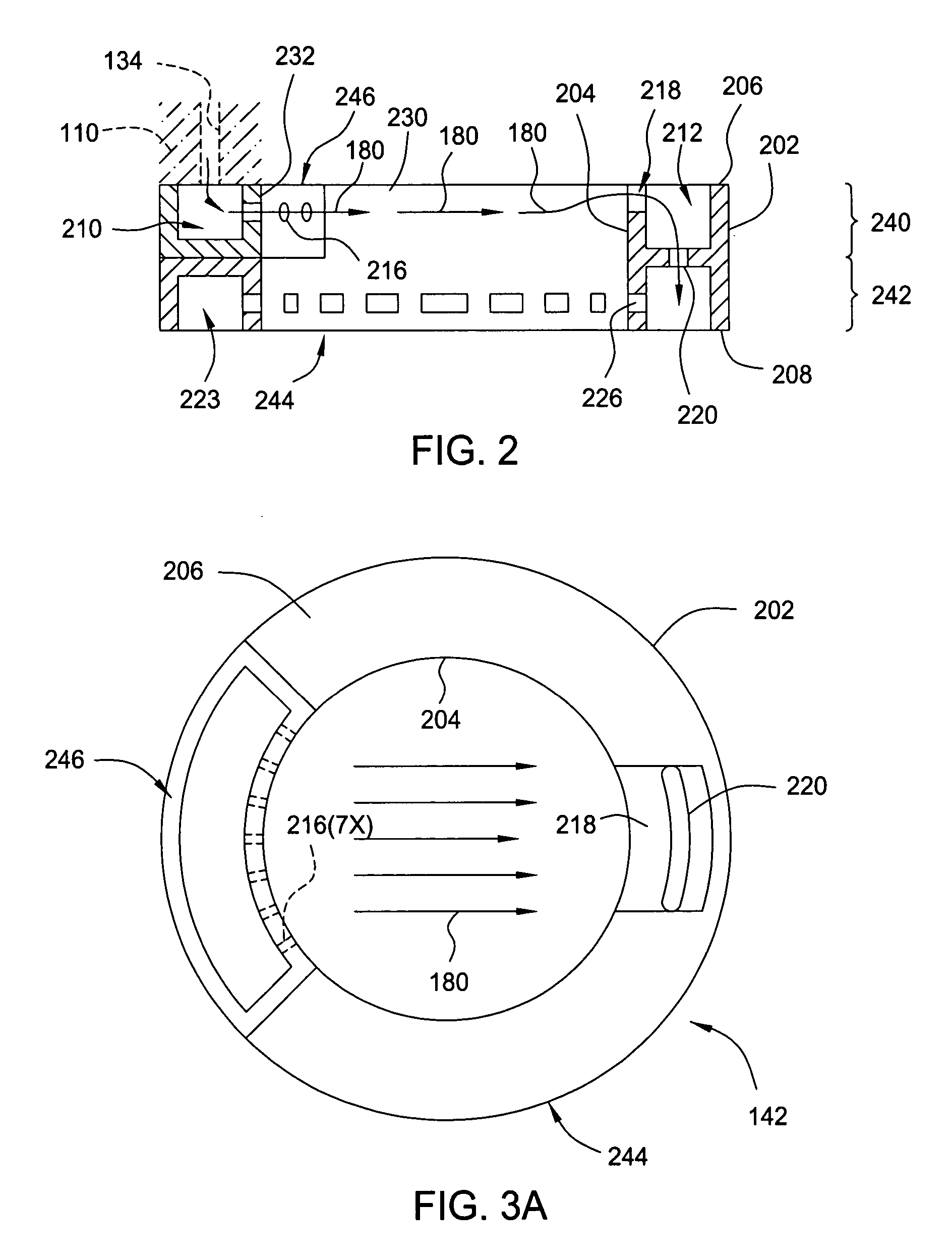
[0023] Embodiments of the invention provide a method for depositing a silicon-containing film, such as silicon nitride and the like, on a substrate. Many of the embodiments described herein may be advantageously performed utilizing temperatures less than about 550 degrees Celsius. Although the invention is described with reference to a single wafer thermal-chemical vapor deposition (processing) chamber 100 illustrated in FIG. 1, it is contemplated that the method may be beneficially practiced in other deposition systems. One processing chamber which may be adapted to benefit from the invention is a SiNgen®Plus chamber, available from Applied Materials, Inc., of Santa Clara, Calif. Moreover, although a silicon nitride deposition process is described below, it is contemplated that the method and apparatus utilized to perform the method may be beneficially adapted to deposit materials in addition to silicon nitride, such as metal silicide and metal nitride, among others.

[0024] Besides...


PUM

PropertyMeasurementUnit
flux of energyaaaaaaaaaa
energyaaaaaaaaaa
wavelengthaaaaaaaaaa

Abstract

Embodiments of the invention generally provide a method for depositing films using photoexcitation. The photoexcitation may be utilized for at least one of treating the substrate prior to deposition, treating substrate and/or gases during deposition, treating a deposited film, or for enhancing chamber cleaning. In one embodiment, a method for depositing silicon and nitrogen-containing film on a substrate includes heating a substrate disposed in a processing chamber, generating a beam of energy of between about 1 to about 10 eV, transferring the energy to a surface of the substrate; flowing a nitrogen-containing chemical into the processing chamber, flowing a silicon-containing chemical with silicon-nitrogen bonds into the processing chamber, and depositing a silicon and nitrogen-containing film on the substrate.

Description

RELATED APPLICATION [0001] This application is related to comtemporality filed U.S. patent application Ser. No. ______, entitled METHOD FOR TREATING SUBSTRATES AND FILMS WITH PHOTOEXCITATION, by Singh, et al., which is incorporated by reference in its entirety.BACKGROUND OF THE INVENTION [0002] 1. Field of the Invention [0003] Embodiments of the invention generally relate to a method for depositing silicon-containing materials, and more particularly, embodiments of the invention relate to chemical vapor deposition techniques for thermally depositing silicon based dielectric materials, such as silicon nitride, using photoexcitation. [0004] 2. Description of the Related Art [0005] Thermal chemical vapor deposition (CVD) of silicon-containing films, such as silicon nitride, is a state of the art, front end process used during semiconductor device manufacturing. For example, in a thermal CVD process for depositing silicon nitride, thermal energy is utilized for breaking one or more feed...

Claims


Application Information

Patent Timeline
Patent Type & Authority Applications(United States)
IPC IPC(8): H01L21/31
CPCC23C16/02C23C16/345H01L21/3185C23C16/56C23C16/482H01L21/0228H01L21/0217
Inventor SEUTTER, SEAN M.SINGH, KAUSHAL K.SMITH, JACOBIYER, R. SURYANARAYANANGHANAYEM, STEVE G.BRAILOVE, ADAMSHYDO, ROBERT JR.MORIN, JEANNOT
Owner APPLIED MATERIALS INC
Why Eureka
Try Eureka