

Semi-transparent TFT array substrate, and semi-transparent liquid crystal display
a liquid crystal display and array substrate technology, applied in semiconductor devices, electrical equipment, instruments, etc., can solve the problems of short circuit between the electrode and the surface of the preventive electrode for contrast reduction, black dot defect generation of the pixel subjected to the short circuit, and short circuit may affect the effect of contrast reduction
- Summary
- Abstract
- Description
- Claims
- Application Information
AI Technical Summary
Benefits of technology
Problems solved by technology
Method used
Image

Examples
first preferred embodiment
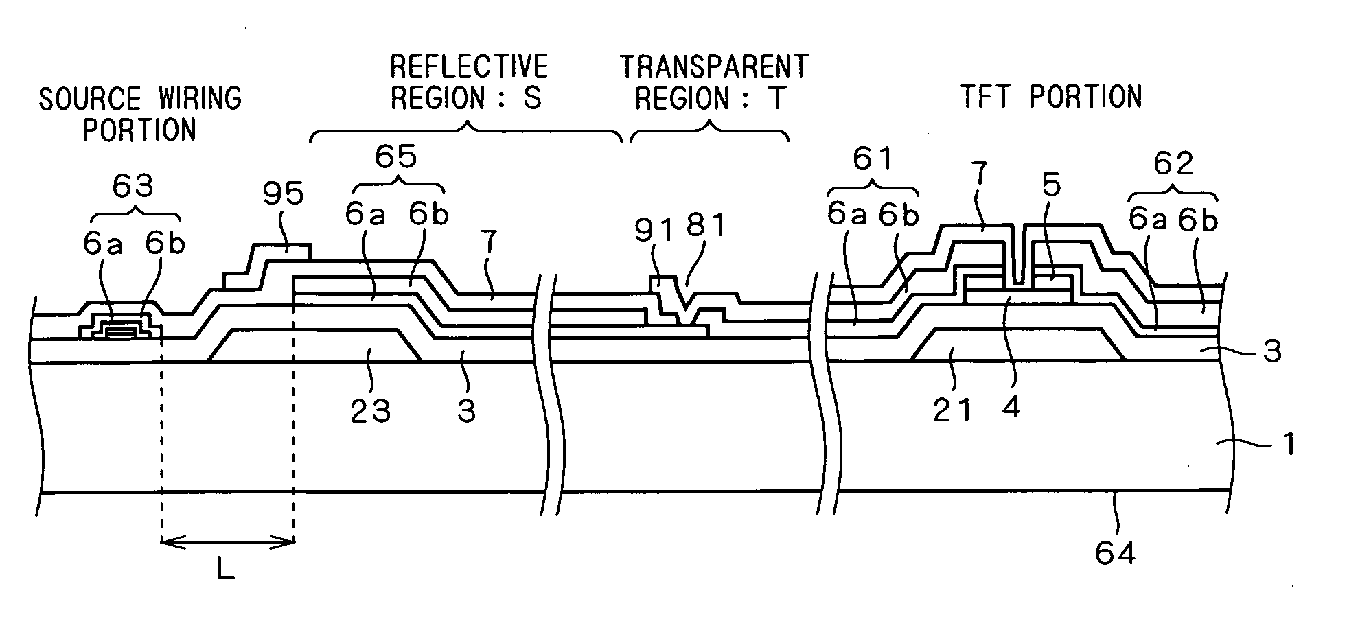
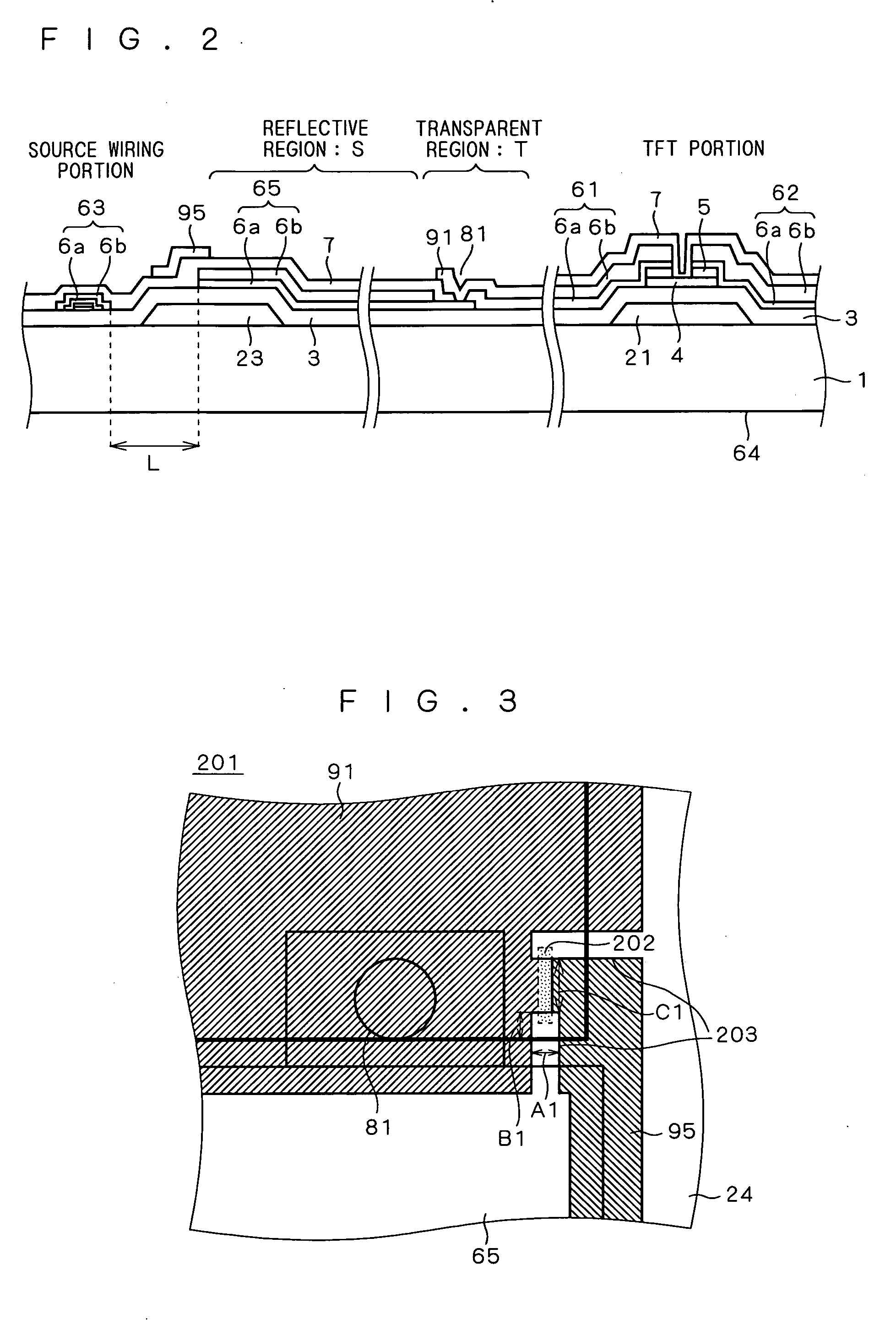
[0023] In a semi-transparent liquid crystal display according to the background art of the present invention, a contrast reduction preventive electrode is provided in the uppermost layer of a reflective region in a TFT array substrate. The contrast reduction preventive electrode is arranged between a source wiring and a reflective pixel electrode.
[0024] An electric field is applied to a liquid crystal layer between the contrast reduction preventive electrode and an opposed electrode by the formation of the contrast reduction preventive electrode. This prevents reflected light from an auxiliary capacitive electrode from appearing on a display screen to thereby provide excellent display characteristic with high reflective contrast.
[0025] On the other hand, due to the arrangement of the contrast reduction preventive electrode in the uppermost layer of the reflective region, the surface of the opposed electrode and the surface of the contrast reduction preventive electrode may be shor...
second preferred embodiment
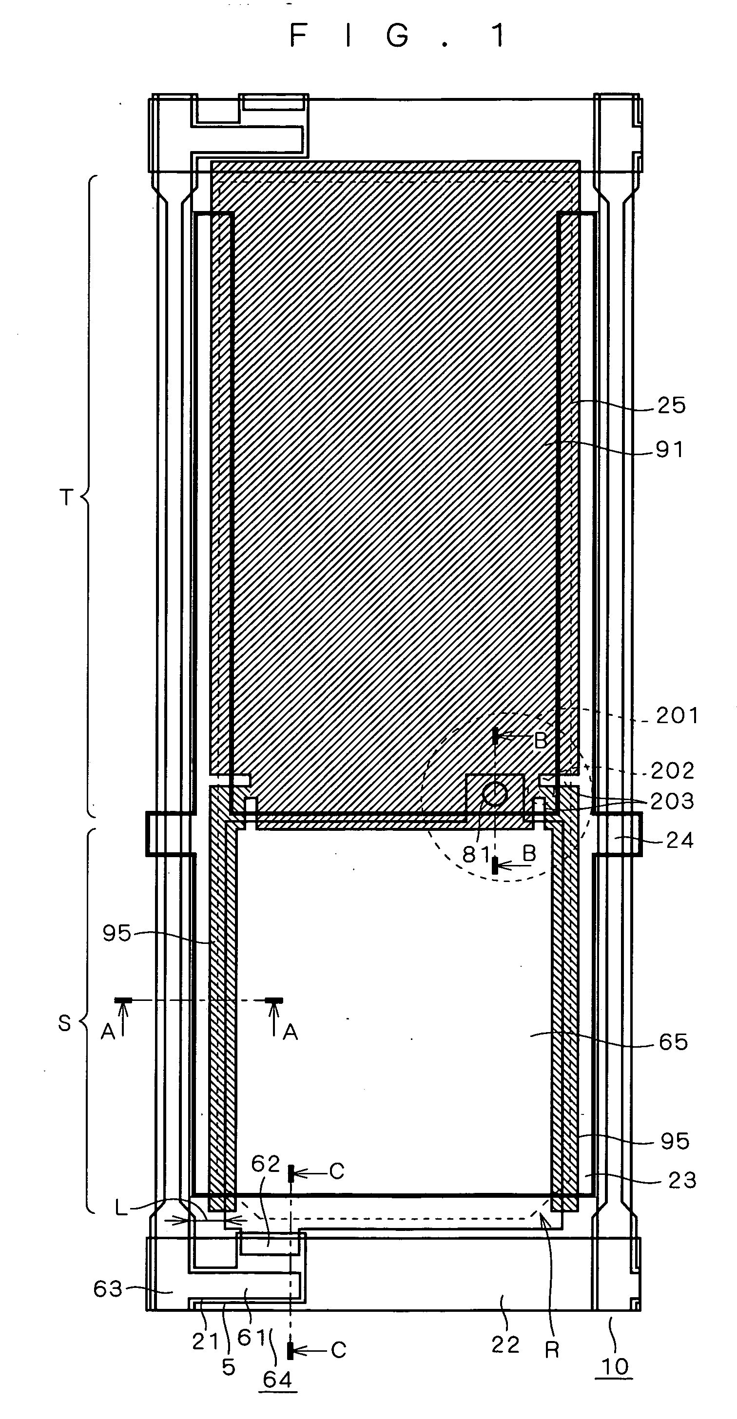
[0104]FIG. 14 is an enlarged top view showing the TFT array substrate 10 constituting a semi-transparent liquid crystal display according to a second preferred embodiment of the present invention.
[0105] In the TFT array substrate 10 of the second preferred embodiment, the pair of slits 203 (see FIGS. 1 and 3) is replaced by slits 205 formed in the auxiliary capacitive wiring 24.
[0106] The connection 202 for connecting the contrast reduction preventive electrode 95 and the transparent pixel electrode 91 is arranged such that the connection 202 corresponds in position to the slits 205 formed in the auxiliary capacitive wiring 24 in plan view.
[0107] Thus the auxiliary capacitive wiring 24 does not overlap the connection 202.
[0108] The other structures are the same as those of the first preferred embodiment, and will not be repeatedly discussed.
[0109] In the steps of manufacturing a panel, laser repair process is performed while viewing an image of the rear surface of the TFT array...
third preferred embodiment
[0116]FIG. 15 is an enlarged top view showing a connection formed in a transparent pixel electrode of the TFT array substrate 10 that constitutes a semi-transparent liquid crystal display according to a third preferred embodiment of the present invention.
[0117] The TFT array substrate 10 of the third preferred embodiment is a combination of the TFT array substrate 10 of the first preferred embodiment and that of the second preferred embodiment. The same structures as those of the first or second preferred embodiment are designated by the same reference numerals, and will not be repeatedly discussed.
[0118] With reference to FIG. 15, the pair of slits 203 is formed in the transparent pixel electrode 91 or the contrast reduction preventive electrode 95. Further, the slits 205 are formed in the auxiliary capacitive wiring 24.
[0119] The TFT array substrate 10 of the third preferred embodiment is formed by incorporating the pair of slits 203 in the transparent pixel electrode 91 or the...
PUM
 Abstract
Description
Claims
Application Information