Semiconductor device

a technology of semiconductor elements and devices, applied in the direction of semiconductor devices, electrical devices, transistors, etc., can solve problems such as impairment of the characteristics of semiconductor elements

Inactive Publication Date: 2006-12-28
SEIKO EPSON CORP
View PDF25 Cites 1 Cited by
  • Summary
  • Abstract
  • Description
  • Claims
  • Application Information

AI Technical Summary

Benefits of technology

[0006] a transistor formed in the semiconductor layer and including a gate insulating layer and a gate electrode, the transistor being a high voltage transistor (or a high breakdown voltage transistor) in which an insulating layer having a thickness greater than the thickness of the gate insulating layer is formed under an end portion of the gate electrode;

Problems solved by technology

In related-art technology, when disposing a semiconductor element such as a MOS transistor under a pad, the characteristics of the semiconductor element may be impaired due to stress during bonding.

Method used


Image

  • Semiconductor device
  • Semiconductor device

Examples


Embodiment Construction

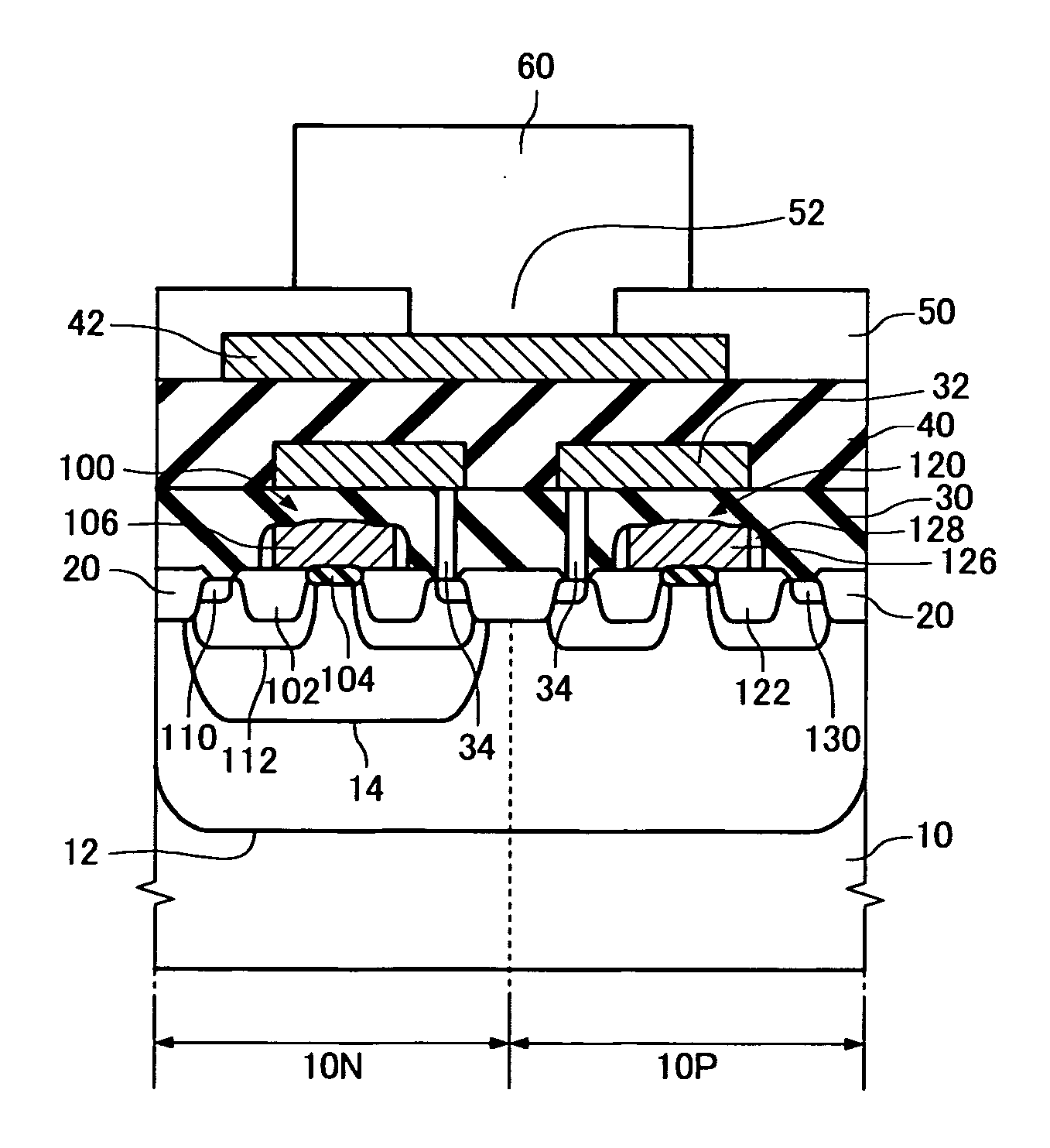
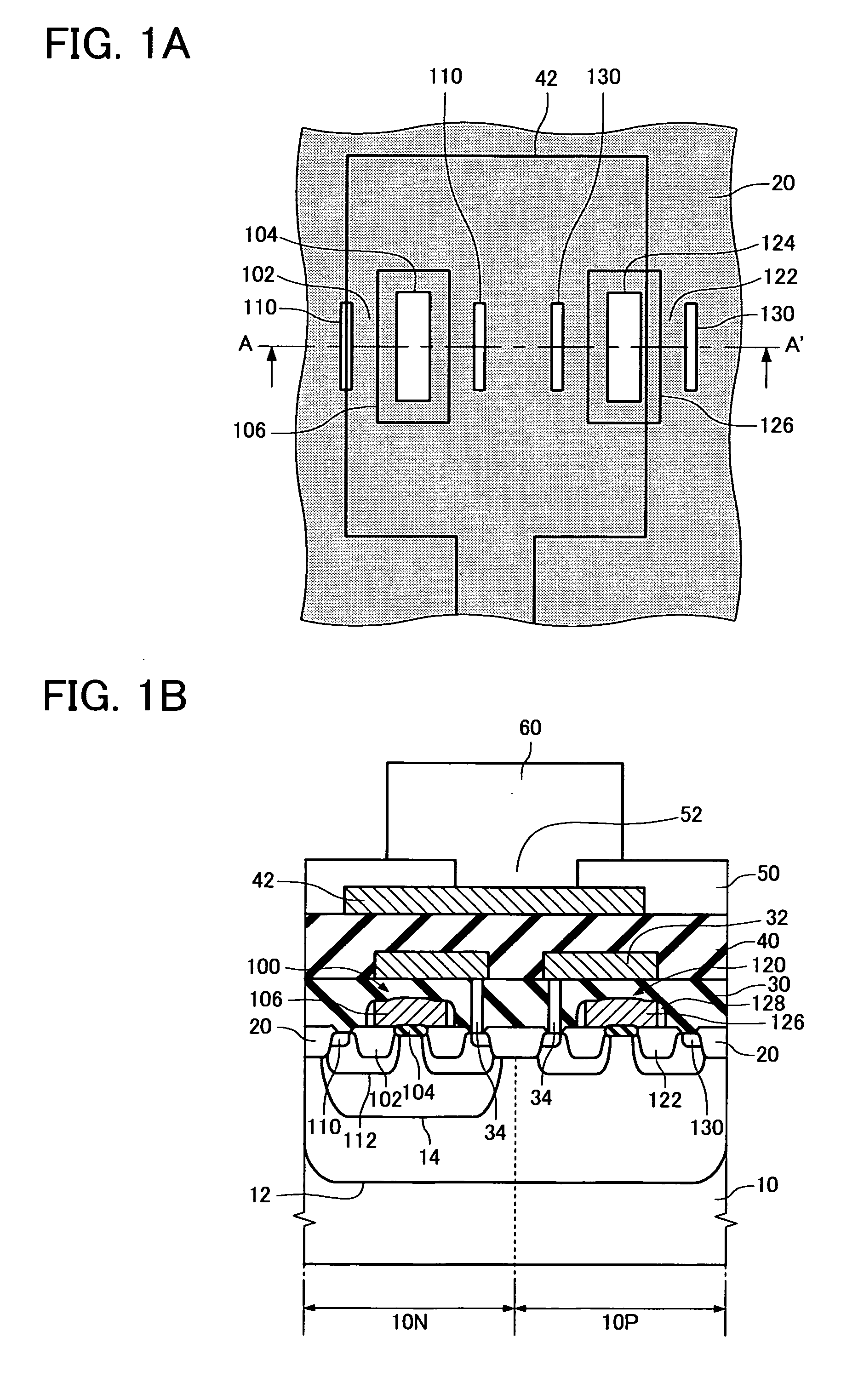
[0010] The invention may provide a highly reliable semiconductor device in which a semiconductor element can be formed under a pad.

[0011] (1) According to one embodiment of the invention, there is provided a semiconductor device comprising:

[0012] a semiconductor layer;

[0013] a transistor formed in the semiconductor layer and including a gate insulating layer and a gate electrode, the transistor being a high voltage transistor in which an insulating layer having a thickness greater than the thickness of the gate insulating layer is formed under an end portion of the gate electrode;

[0014] an interlayer dielectric formed above the transistor; and

[0015] an electrode pad formed above the interlayer dielectric and positioned over at least part of the gate electrode when viewed from a top side.

[0016] In the semiconductor device according to this embodiment, the transistor is formed under the electrode pad, and the electrode pad is positioned over at least part of the gate electrode o...


PUM


Abstract

A semiconductor device including: a semiconductor layer; a transistor formed in the semiconductor layer and including a gate insulating layer and a gate electrode, the transistor being a high voltage transistor in which an insulating layer having a thickness greater than the thickness of the gate insulating layer is formed under an end portion of the gate electrode; an interlayer dielectric formed above the transistor; and an electrode pad formed above the interlayer dielectric and positioned over at least part of the gate electrode when viewed from a top side.

Description

[0001] Japanese Patent Application No. 2005-183365, filed on Jun. 23, 2005, is hereby incorporated by reference in its entirety. BACKGROUND OF THE INVENTION [0002] The present invention relates to a semiconductor device. [0003] In related-art technology, when disposing a semiconductor element such as a MOS transistor under a pad, the characteristics of the semiconductor element may be impaired due to stress during bonding. Therefore, the pad formation region and the semiconductor element formation region of a semiconductor chip are separated when viewed from the top side. However, since the semiconductor chip has been reduced in size and increased in degree of integration, disposition of the semiconductor element under the pad has been demanded. JP-A-2002-319587 discloses such technology, for example. SUMMARY [0004] According to one aspect of the invention, there is provided a semiconductor device comprising: [0005] a semiconductor layer; [0006] a transistor formed in the semiconduc...

Claims


Application Information

Patent Timeline
Patent Type & Authority Applications(United States)
IPC IPC(8): H01L31/00
CPCH01L21/823462H01L27/088H01L29/78H01L29/1041H01L29/42368H01L29/1037H01L24/05H01L2224/05022H01L2224/05166H01L2224/05184H01L2224/05567H01L2224/05568H01L2224/0558H01L2224/05644H01L2224/05666H01L2224/05684H01L2224/11H01L2924/00014H01L2924/01074H01L2924/013H01L21/28H01L21/3205
Inventor SHINDO, AKINORITAGAKI, MASATOSHIKURITA, HIDEAKI
Owner SEIKO EPSON CORP
Why Eureka
Try Eureka