
Liquid crystal display device and method of manufacturing the same

a liquid crystal display and display device technology, applied in static indicating devices, instruments, non-linear optics, etc., can solve the problems of flicker or image-sticking, tn lcd, and disadvantages in terms of miniaturization and portability, and achieve the effect of accurately applying pixel voltage and eliminating flicker and image-sticking

Inactive Publication Date: 2006-12-28
LG DISPLAY CO LTD
View PDF6 Cites 83 Cited by
  • Summary
  • Abstract
  • Description
  • Claims
  • Application Information

AI Technical Summary

Benefits of technology

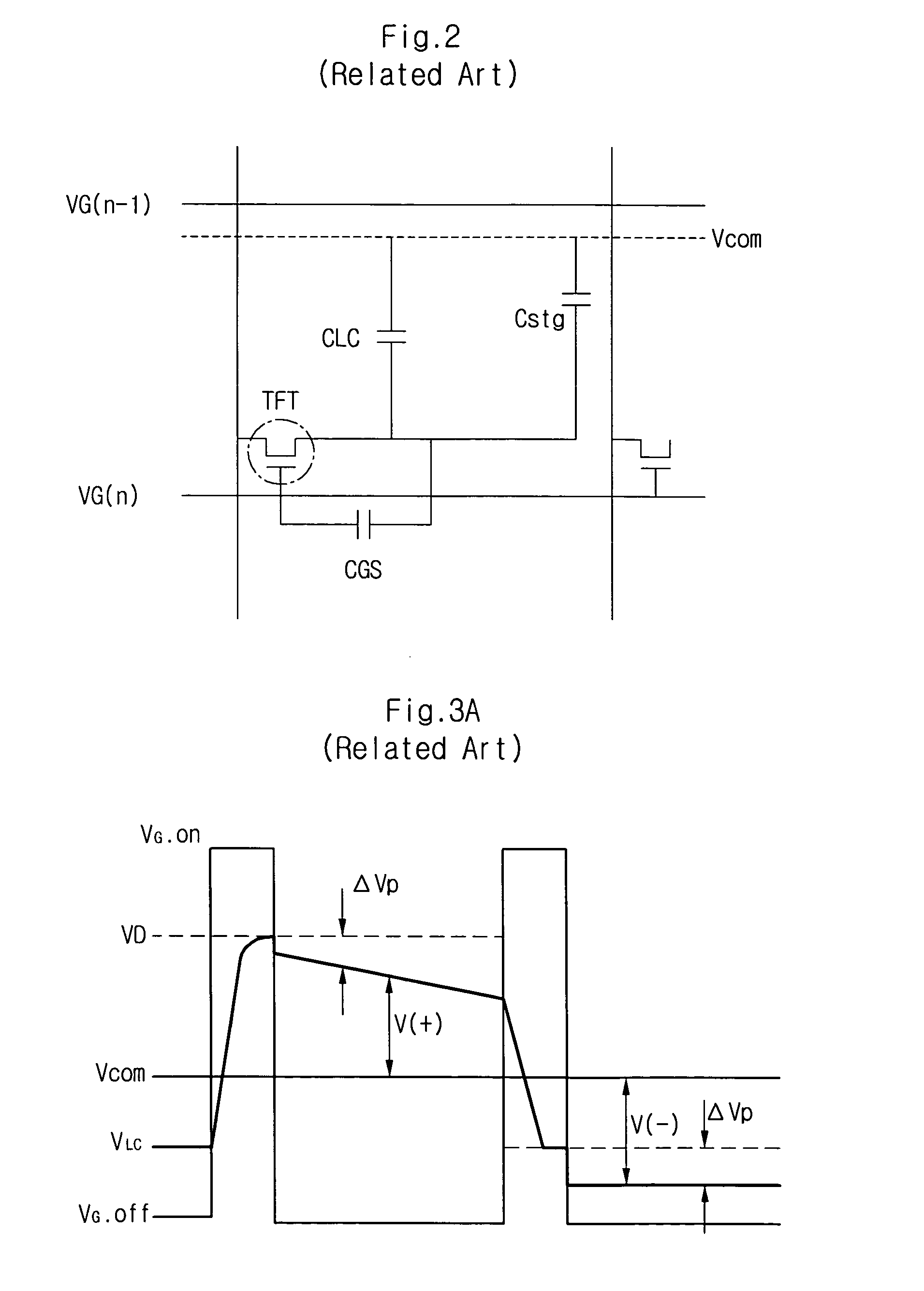
[0030] The LCD may be capable of eliminating flicker and image-sticking, and may be able to apply accurately a pixel voltage in a white state or a black state by shifting a common voltage to correspond to a level shift voltage (ΔVP) generated at a pixel region.

Problems solved by technology

However, CRTs also have disadvantages in terms of miniaturization and portability.
The TN LCD, however, has a very narrow viewing angle.
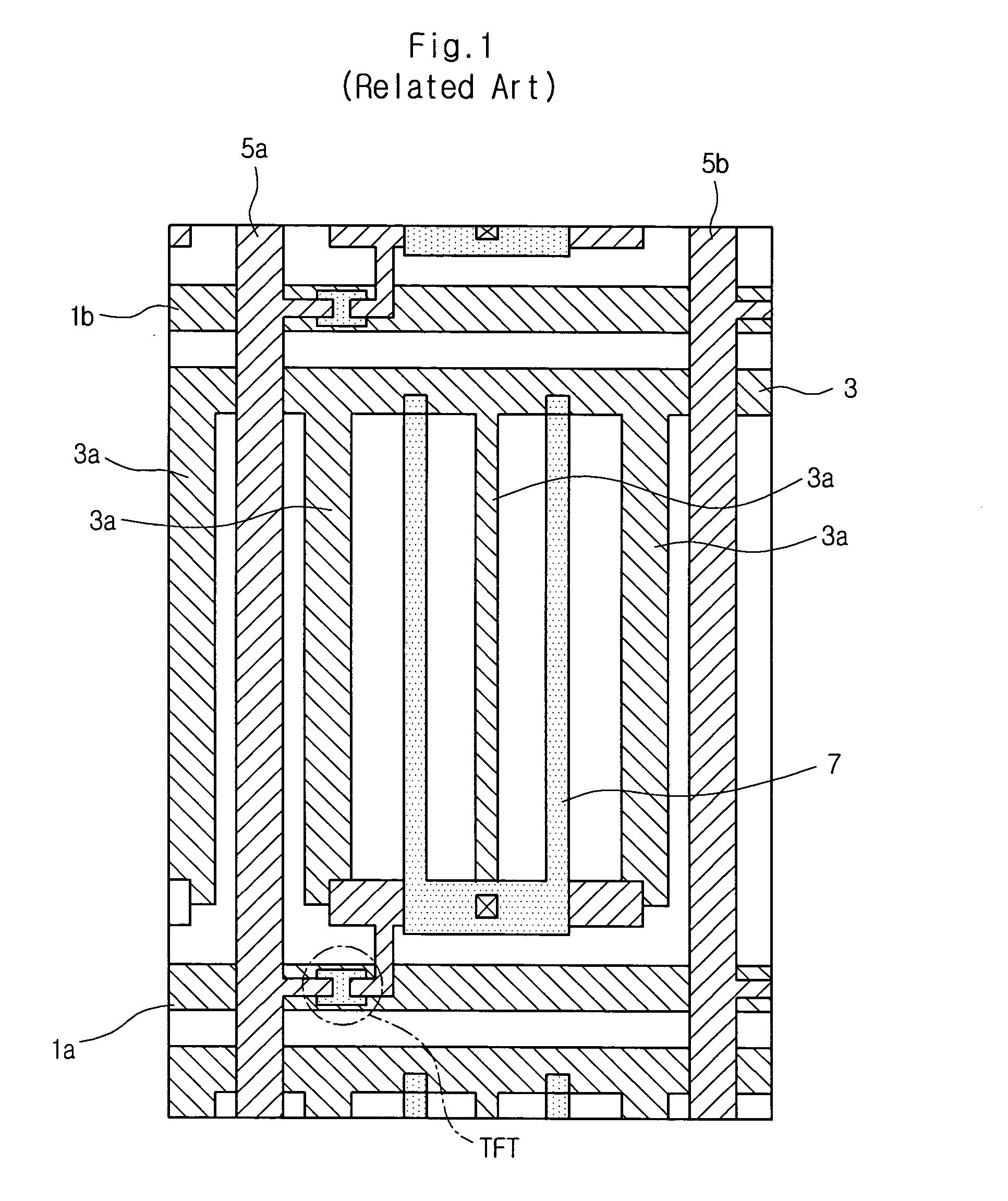
In the low region, a pixel voltage V(−) lower than an original voltage is formed due to the level shift voltage ΔVP, causing flicker or image-sticking.
That is, even if the white state voltage is applied, the accurate white voltage is not exhibited, resulting in failure.
In the low region, a pixel voltage V(−) lower than an original voltage is formed due to the level shift voltage ΔVP, causing flicker or image-sticking.

Method used


Image

  • Liquid crystal display device and method of manufacturing the same
  • Liquid crystal display device and method of manufacturing the same
  • Liquid crystal display device and method of manufacturing the same

Examples


Embodiment Construction

[0054] Reference will now be made in detail to the preferred embodiments of the LCD device, examples of which are illustrated in the accompanying drawings. Wherever possible, the same reference numbers will be used throughout the drawings to refer to the same or like parts.

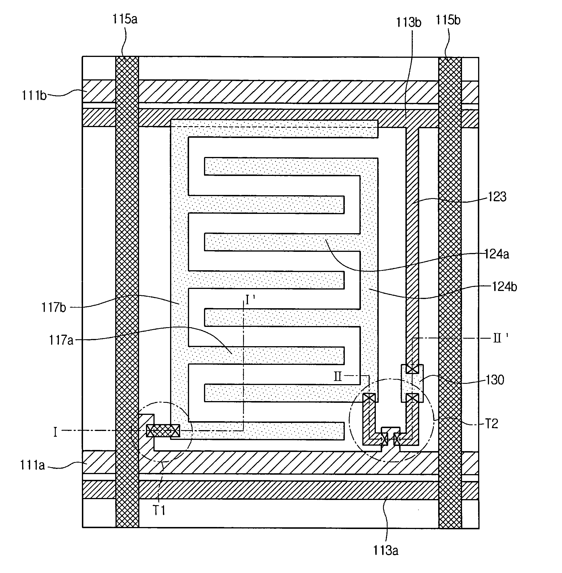
[0055]FIG. 4A is a plan view of a pixel structure of an IPS LCD according to one embodiment.

[0056] Referring to FIG. 4A, gate lines 111a and 111b for applying driving signals are positioned parallel to each other and perpendicular to data lines 115a and 115b for applying data signals. This configuration defines a unit pixel region. A first switch, such as, for example, a thin film transistor (TFT), acting as a switching element is positioned adjacent to the intersection of the gate line 111a and the data line 115a. This switch will be referred to as TFT T1. A second switch, which will be referred to as TFT T2, faces the first TFT T1 and is positioned adjacent to the intersection of the gate line 111a and the dat...


PUM


Abstract

An LCD includes a first gate line and a second gate line disposed parallel to each other and perpendicular to a first data line and a second data line, thereby defining a unit pixel region, a first common line disposed parallel to the gate lines, a second common line extending from the first common line, a pixel bar and pixel electrodes disposed in the unit pixel region and electrically connected to a first TFT, a second TFT electrically connected to the second common line, a common bar and common electrodes electrically connected to the second TFT, the common electrodes being disposed alternately with the pixel electrodes.

Description

TECHNICAL FIELD [0001] The present application relates to a liquid crystal display device, and more particularly, to a liquid crystal display device capable of enhancing image quality by compensating a level shift voltage generated at a pixel region, and a method of manufacturing the same. BACKGROUND [0002] In today's information-driven society, the importance of liquid crystal display device (LCD) technology is increasing. Cathode ray tube (CRT) devices have been widely used to date and have many advantages in terms of performance and price. However, CRTs also have disadvantages in terms of miniaturization and portability. [0003] In order to replace the CRT, a lightweight and slim LCD that can provide high brightness, large-size, low power consumption, and low cost has been developed. [0004] A widely-used twist nematic (TN) LCD includes a common electrode and a pixel electrode that are formed on a top substrate and a bottom substrate, respectively. An electric field is generated be...

Claims


Application Information

Patent Timeline
IPC IPC(8): G02F1/1343
CPCG02F1/134363G02F1/13624G02F1/136286G09G2310/0289G09G3/3655G09G2300/0434G02F2201/124G02F1/1343
Inventor HOESUP, SOH
Owner LG DISPLAY CO LTD
Learn More