Electrostatic chuck, wafer processing apparatus and plasma processing method

a plasma processing and electrostatic chuck technology, applied in the direction of semiconductor/solid-state device manufacturing, basic electric elements, electric apparatus, etc., can solve the problems of poor reproducibility among wafers, method is not suitable for changing wafer temperature, and the need for dimensional accuracy in processing has become more and more severe, so as to reduce manufacturing costs, simple and accurate prediction of wafer temperature, the effect of good responsivity

a plasma processing and electrostatic chuck technology, applied in the direction of semiconductor/solid-state device manufacturing, basic electric elements, electric apparatus, etc., can solve the problems of poor reproducibility among wafers, method is not suitable for changing wafer temperature, and the need for dimensional accuracy in processing has become more and more severe, so as to reduce manufacturing costs, simple and accurate prediction of wafer temperature, the effect of good responsivity

US20060291132A1Inactive Publication Date: 2006-12-28HITACHI HIGH-TECH CORP

Image

  • Electrostatic chuck, wafer processing apparatus and plasma processing method
  • Electrostatic chuck, wafer processing apparatus and plasma processing method
  • Electrostatic chuck, wafer processing apparatus and plasma processing method

Examples


Embodiment Construction

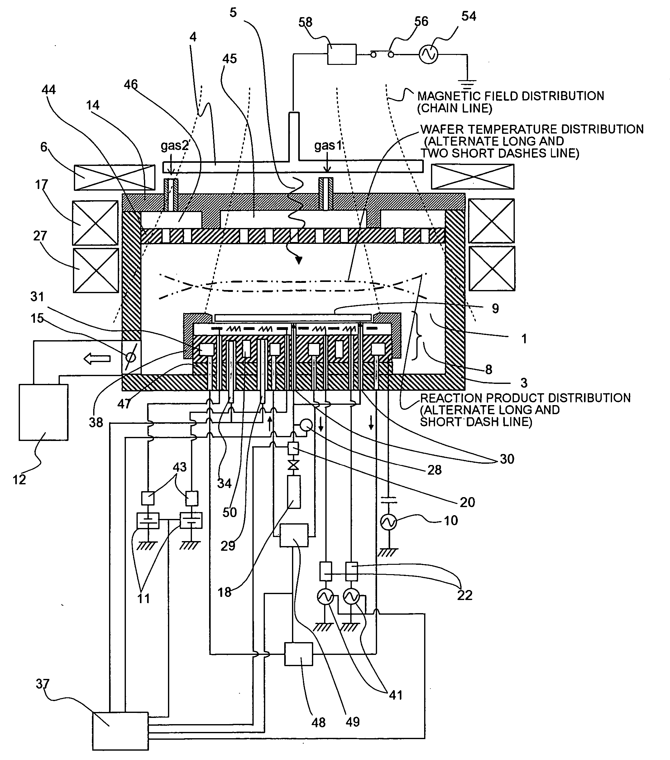
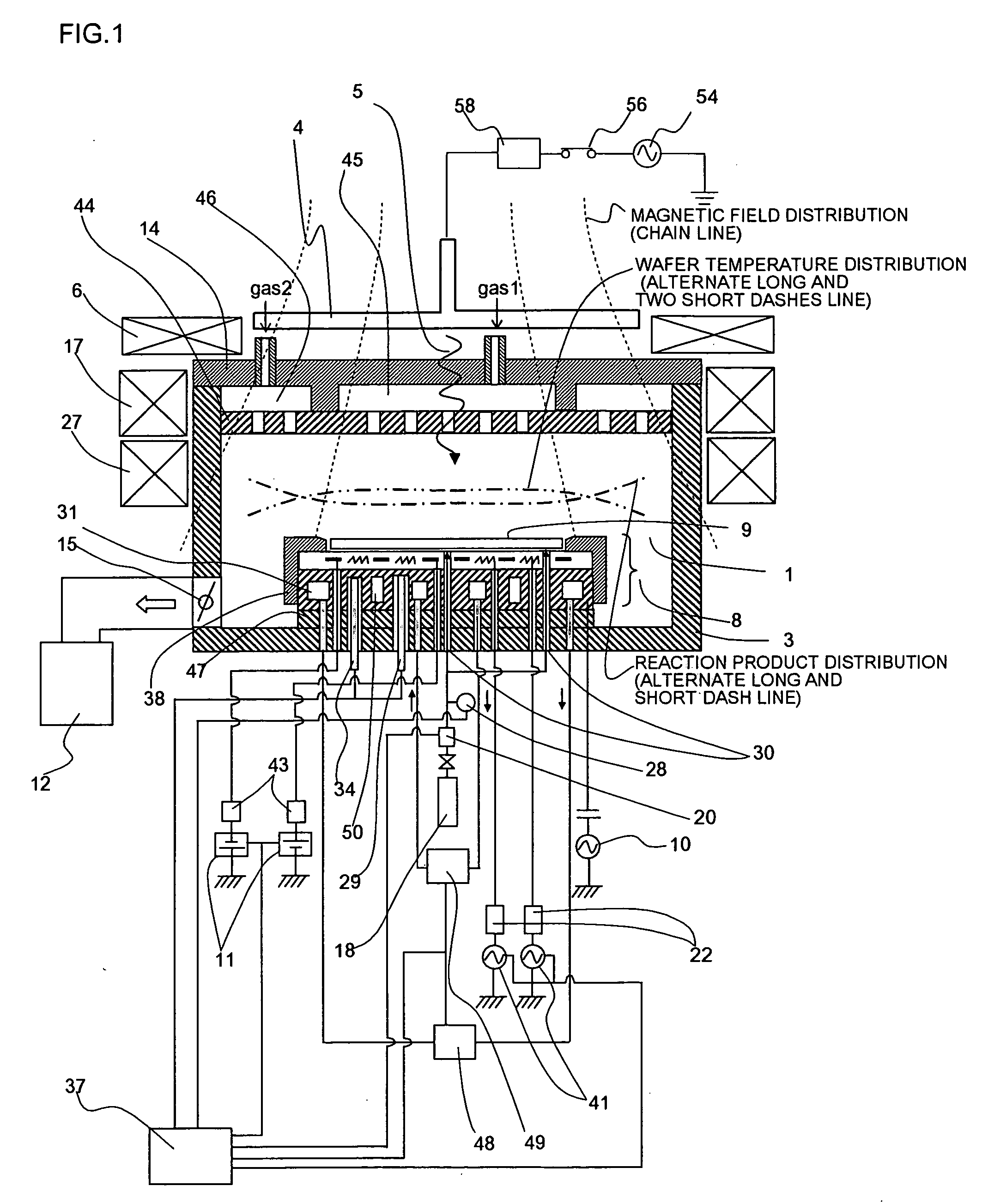
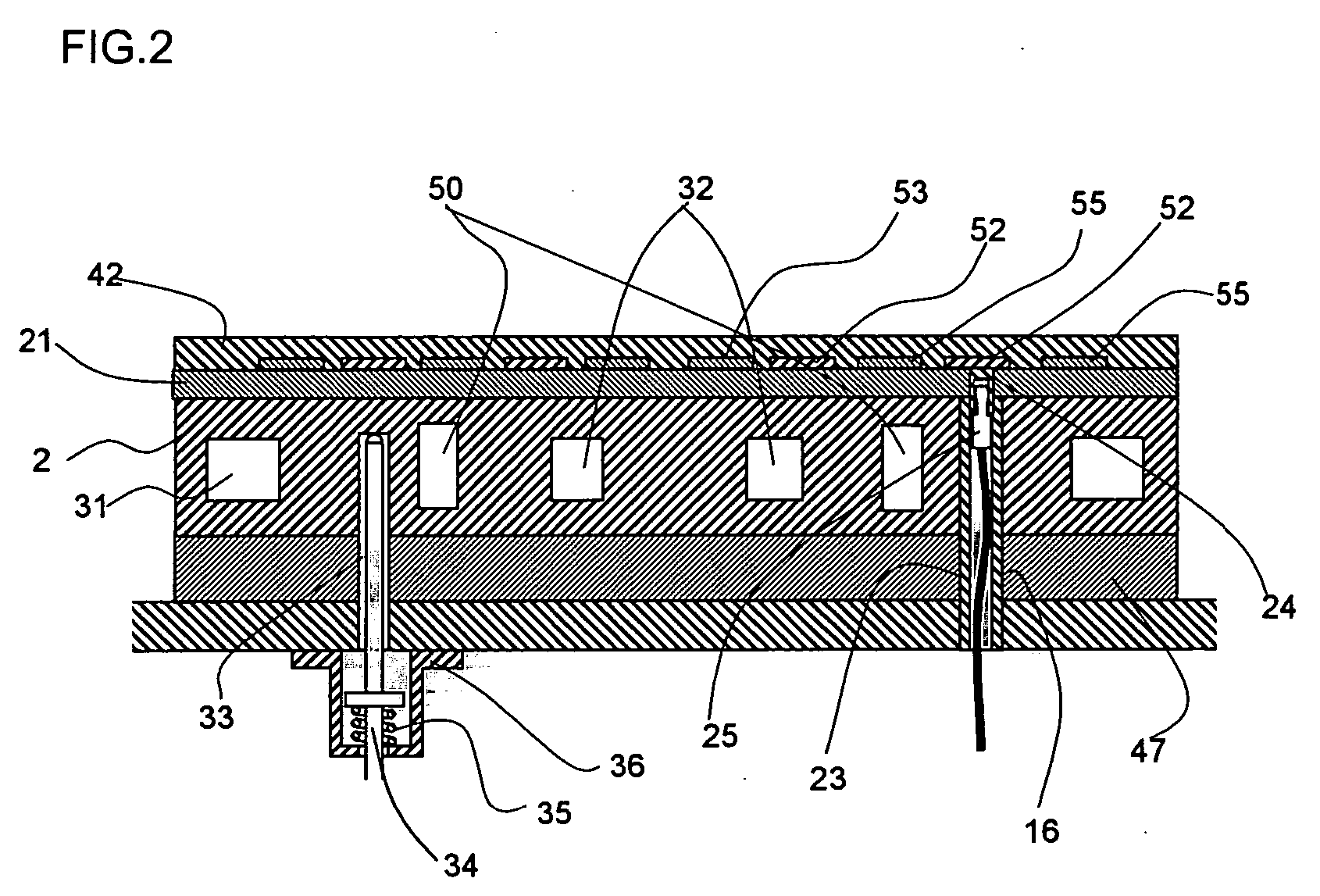
[0027] FIGS. 1 to 3 show a first embodiment of the present invention applied to a UHF plasma processing apparatus. FIG. 1 is a schematic illustration showing the general system configuration including an electrostatic chuck of the first embodiment, and this example can explain the technical philosophy of the present invention. FIG. 2 is a detailed sectional view to explain a power feed section to a temperature monitor, a heater and an electrode of the electrostatic chuck of the first embodiment. FIG. 3 is a pattern diagram of the heater and electrode of the electrostatic chuck. First, with reference to FIGS. 1, 2 and 3, the technical philosophy and general system configuration of the present invention will be described.

[0028] A shower head plate 44 made of quartz and a treatment chamber lid 14 made of quartz are installed in an upper part of a vacuum chamber 3. Between the treatment chamber lid 14 and the shower head plate 44, there is provided a space which uniformly disperses a t...


PUM


Abstract

An electrostatic chuck which is built in a heater and can change, at a high speed, the temperature distribution of a wafer being processed by a plasma is provided at low cost. Also, there is provided a processing method which realizes uniform etching by suppressing CD variations in the plane of the wafer even when etching conditions change. The electrostatic chuck includes a base material in which multiple coolant grooves are formed, a high resistance layer which is formed on the base material, multiple heaters which are formed by thermally spraying conductors within the high resistance layer, multiple electrostatic chuck electrodes which are formed similarly by thermally spraying conductors within the high resistance layer, and temperature measuring means, and adjusts outputs of the heaters on the basis of temperature information of the temperature measuring means.

Description

[0001] The present application is based on and claims priority of Japanese patent application No. 2006-035034 filed on Feb. 13, 2006, the entire contents of which are hereby incorporated by reference. BACKGROUND OF THE INVENTION [0002] 1. Field of the Invention [0003] The present invention relates to an etching technique of a semiconductor wafer and, more particularly, to a wafer processing apparatus which continuously processes a semiconductor wafer. [0004] 2. Description of the Related Art [0005] In recent years, circuit patterns processed in a semiconductor wafer have kept on becoming increasingly fine owing to high-density designs of semiconductor elements and required dimensional accuracies in processing have become more and more severe. Under such circumstances, the temperature control of a wafer (semiconductor wafer) being processed becomes a very important matter. [0006] For example, in etching a wafer by using a plasma, usually, bias voltage is applied to the wafer and ions...

Claims


Application Information

Patent Timeline
28 Dec 2006
Publication
US20060291132A1
IPC
H01T23/00
CPC
H01L21/67103; H01L21/6831; H01L21/67109; H01L21/3065
Inventors
KANNO, SEIICHIRO; TSUBONE, TSUNEHIKO