Wafer processing method

a processing method and wafer technology, applied in welding/soldering/cutting articles, manufacturing tools, solid-state devices, etc., can solve the problems of difficult to form via-holes with a diameter of 30 to 500 m, wafers are easily broken, and are difficult to handle during conveyance, so as to maintain the effect of stiffness

Active Publication Date: 2006-12-28
DISCO CORP
View PDF3 Cites 24 Cited by
  • Summary
  • Abstract
  • Description
  • Claims
  • Application Information

AI Technical Summary

Benefits of technology

[0007] It is an object of the present invention to provide a wafer processing method capable of forming through-holes (via-holes) easily without causing any trouble in the handling of a wafer during its conveyance.
[0012] According to the present invention, since the recess is formed by removing an area, which corresponds to the device area, in the back surface of the wafer and the thickness of the device area is reduced to a predetermined value by carrying out the reinforcement forming step, a via-hole can be easily formed in the electrodes of the wafer in the via-hole forming step. Further, since an area corresponding to the extra area is kept in the wafer which has been subjected to the reinforcement forming step to form an annular reinforcement so as to maintain its stiffness, it is not broken during conveyance and in the subsequent steps such as a step of forming an insulating film in the via-holes, a step of burying an electrode in the via-holes, a testing step and a dicing step.

Problems solved by technology

Since the thickness of the wafer before its back surface is ground to a predetermined thickness is about 700 μm, however, it is very difficult to form via-holes having a diameter of 30 to 500 μm.
Further, when via-holes are perforated after the back surface of the wafer is ground to a predetermined thickness (for example, 30 to 50 μm), they can be perforated relatively easily but the wafer is easily broken because of its thin thickness and is difficult to handle during conveyance because it curves.
However, when the electrode is exposed by grinding the back surface of the wafer, problems arise that the electrode may stretch like whiskers due to its ductility to cause a short-circuit with an adjacent electrode, or a copper ion may enter the inside from the back surface of the wafer to reduce the quality of a device.

Method used


Image

  • Wafer processing method
  • Wafer processing method
  • Wafer processing method

Examples


Embodiment Construction

[0022] Preferred embodiments of the present invention will be described in more detail hereinunder with reference to the accompanying drawings.

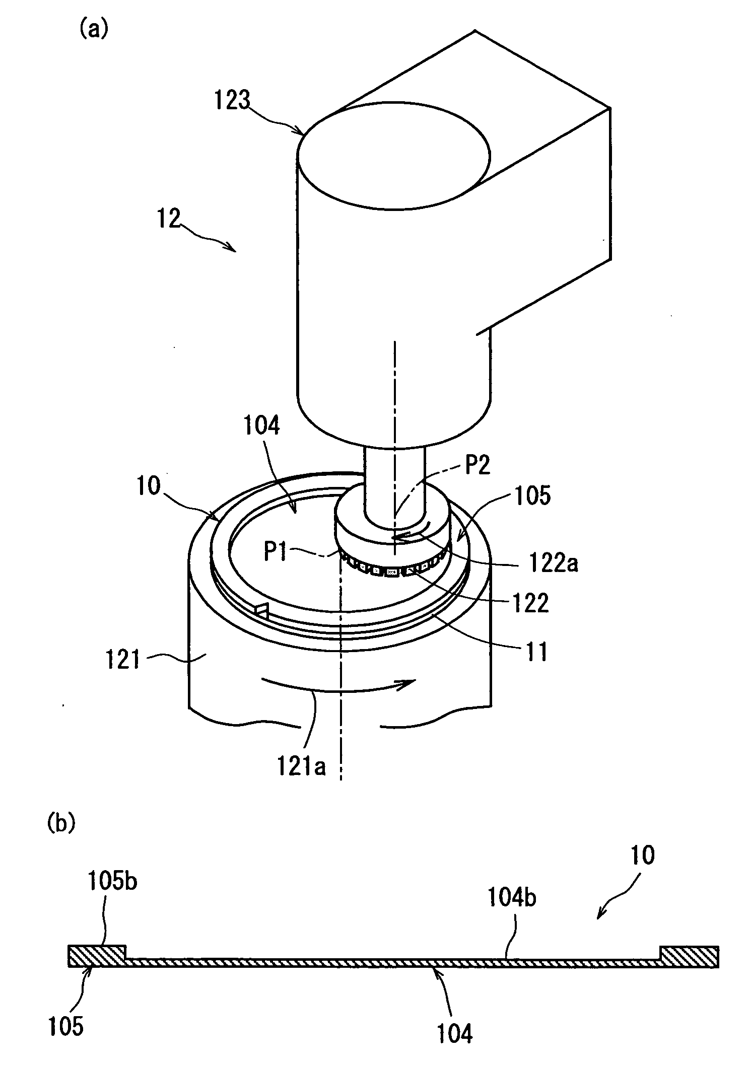
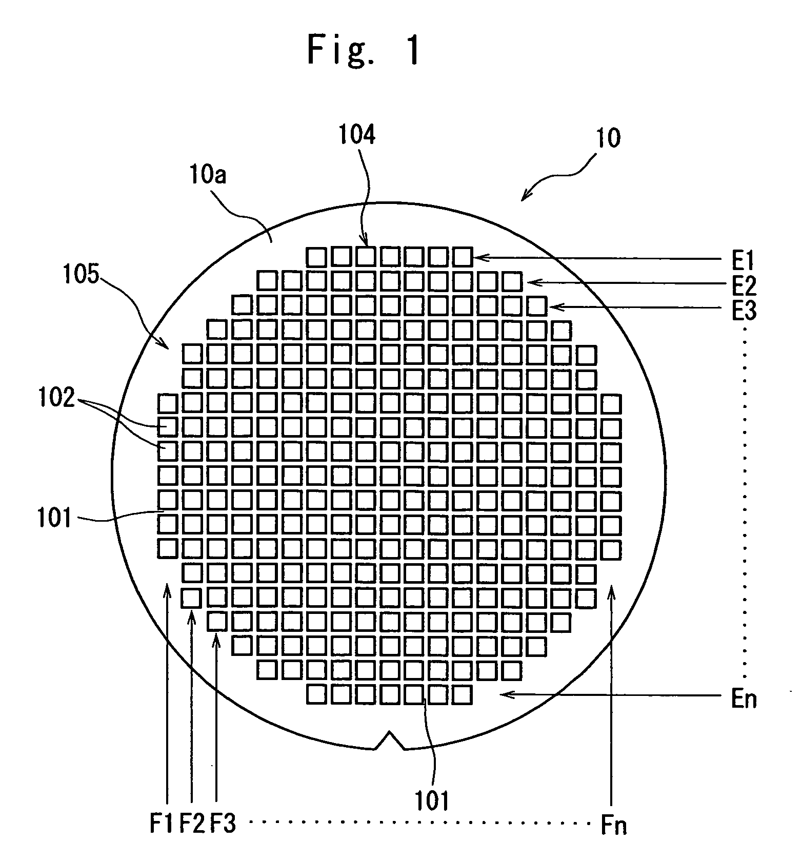
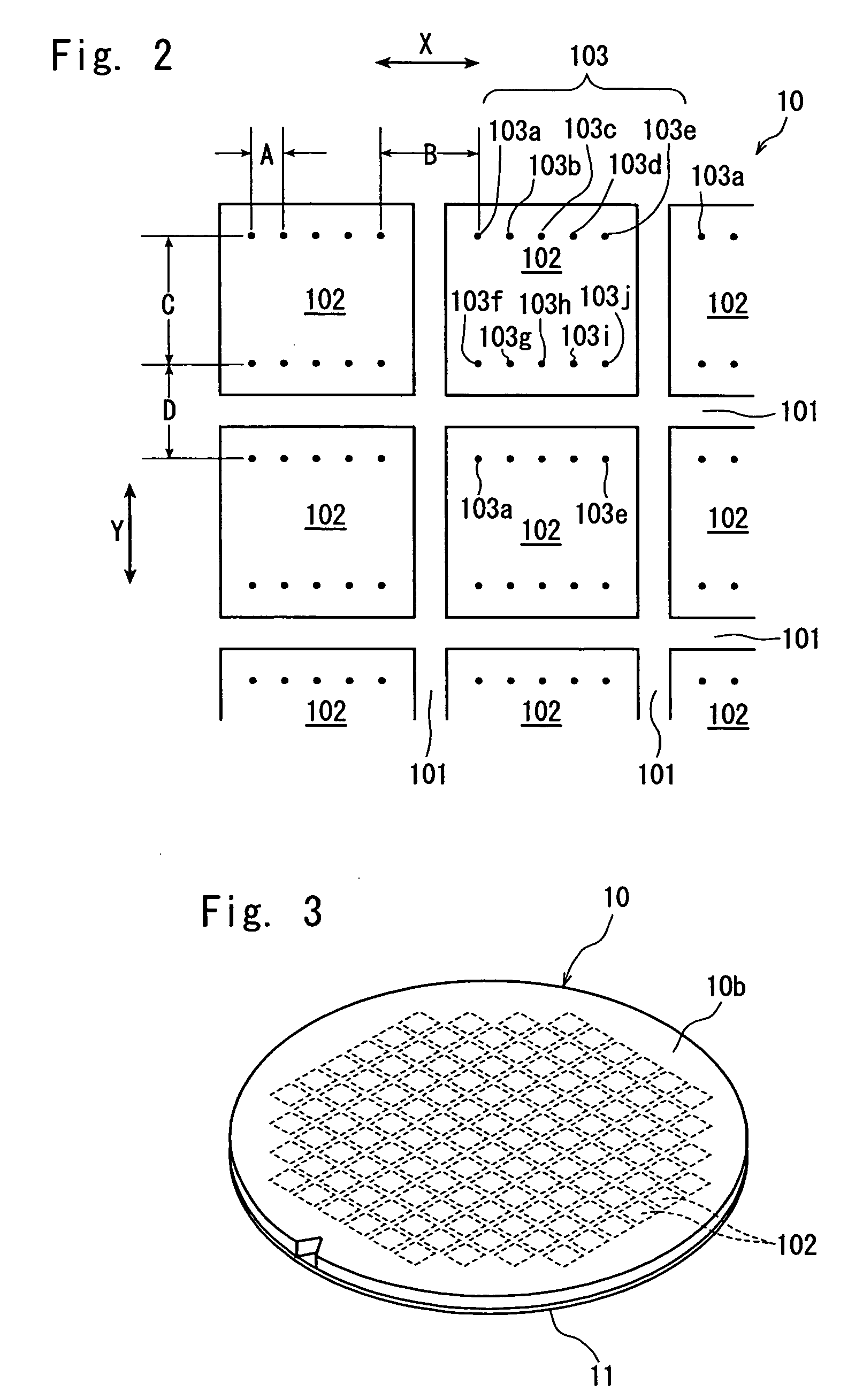
[0023]FIG. 1 is a plan view of a semiconductor wafer as a wafer to be processed according to the present invention. The semiconductor wafer 10 shown in FIG. 1 is, for example, a silicon wafer having a thickness of 700 μm, a plurality of streets 101 are formed on the front surface 10a, and a device 102 such as IC or LSI is formed in a plurality of areas sectioned by the plurality of streets 101. These devices 102 are the same in constitution. A plurality of electrodes 103 (103a to 103j) are formed on the surface of each device 102, as shown in FIG. 2. In the illustrated embodiment, electrodes 103a and 103f, electrodes 103b and 103g, electrodes 103c and 103h, electrodes 103d and 103i, and electrodes 103e and 103j are at the same positions in the X direction. A via-hole is formed in each of the plurality of electrodes 103 (103a to 103j). The in...


PUM

PropertyMeasurementUnit
diameteraaaaaaaaaa
thicknessaaaaaaaaaa
thicknessaaaaaaaaaa

Abstract

A method of processing a wafer having a device area where a plurality of devices are formed on the front surface and an extra area surrounding the device area and comprising electrodes which are formed in the device area, comprising: a reinforcement forming step for removing an area, which corresponds to the device area, in the back surface of the wafer to reduce the thickness of the device area to a predetermined value and keeping an area, which corresponds to the extra area, in the back surface of the wafer to form an annular reinforcement; and a via-hole forming step for forming a via-hole in the electrodes of the wafer which has been subjected to the reinforcement forming step.

Description

FIELD OF THE INVENTION [0001] The present invention relates to a method of processing a wafer having a plurality of devices formed on the front surface thereof and, more specifically, to a method of processing a wafer to form via-holes at positions where electrodes of a plurality of devices are formed. DESCRIPTION OF THE PRIOR ART [0002] In the manufacturing process of a semiconductor device, a plurality of areas are sectioned by dividing lines called “streets” arranged in a lattice pattern on the front surface of a substantially disk-like semiconductor wafer, and a device such as IC or LSI is formed in each of the sectioned areas. Individual semiconductor chips are manufactured by grinding the back surface of this semiconductor wafer to form a determined thickness and then, cutting the semiconductor wafer along the dividing lines to divide it into the areas each having a device formed thereon. [0003] To reduce the size and increase the number of functions of an apparatus, a module ...

Claims


Application Information

Patent Timeline
Patent Type & Authority Applications(United States)
IPC IPC(8): H01L21/30B23K26/382H01L21/02H01L25/07H01L25/18
CPCB23K26/381B23K26/421H01L21/304H01L21/3043H01L21/67132H01L21/6836Y10S438/959H01L2221/68327H01L24/05B23K26/4075Y10S438/977Y10S438/94H01L21/76898B23K26/40B23K26/382B23K26/60B23K2103/50H01L2924/14H01L2924/00
Inventor KAJIYAMA, KEIICHIKONDO, KOICHIKANEUCHI, YASUOMI
Owner DISCO CORP
Why Eureka
Try Eureka