Scalable uniform thermal plate

a technology of uniform thermal plate and thermal plate, applied in the direction of instruments, coatings, photomechanical treatment, etc., can solve the problems of increasing line width, affecting device performance, and not being able to remove portions of photoresist layer as desired, so as to reduce unwanted processing variation, promote scalability of temperature control apparatus, and uniform temperature control over various regions

Inactive Publication Date: 2007-01-04
SOKUDO CO LTD
View PDF7 Cites 17 Cited by
  • Summary
  • Abstract
  • Description
  • Claims
  • Application Information

AI Technical Summary

Benefits of technology

[0007] Embodiments of methods and apparatuses in accordance with the present invention regulate temperature of a processed workpiece by flowing a thermal control fluid from a thermal source to a thermal drain, in a direction substantially normal to a plane occupied by a substrate. This flow orientation results in any temperature gradient in the thermal control fluid also being positioned normal to the plane of the workpiece, thereby reducing unwanted processing variation attributable to an in-plane temperature gradient. The thermal control fluid is flowed from a common source to a region proximate to the workpiece in a plurality of pixel like regions, in order to ensure uniform temperature control over various regions of the workpiece. The use of such pixel-like regions promotes scalability of the temperature control apparatus.

Problems solved by technology

The precision with which the patterns are developed on the semiconductor substrate impacts the CDs present on the substrate, likely impacting device performance.
Overdevelopment may result in an increase in linewidths, whereas underdevelopment may result in portions of the photoresist layer not being removed as desired.
Temperature nonuniformities can result in undesirable variation in resist processing, affecting consistency in structure and operation of active electrical devices fabricated on the same workpiece.

Method used


Image

  • Scalable uniform thermal plate
  • Scalable uniform thermal plate
  • Scalable uniform thermal plate

Examples


Embodiment Construction

[0035] According to the present invention, techniques related to the field of semiconductor processing equipment are provided. One particular embodiment in accordance with the present invention relates to processing a semiconductor workpiece with resist material. Merely by way of example, the method and apparatus have been applied to processing a semiconductor workpiece with resist. It should be recognized that the invention has a much broader range of applicability.

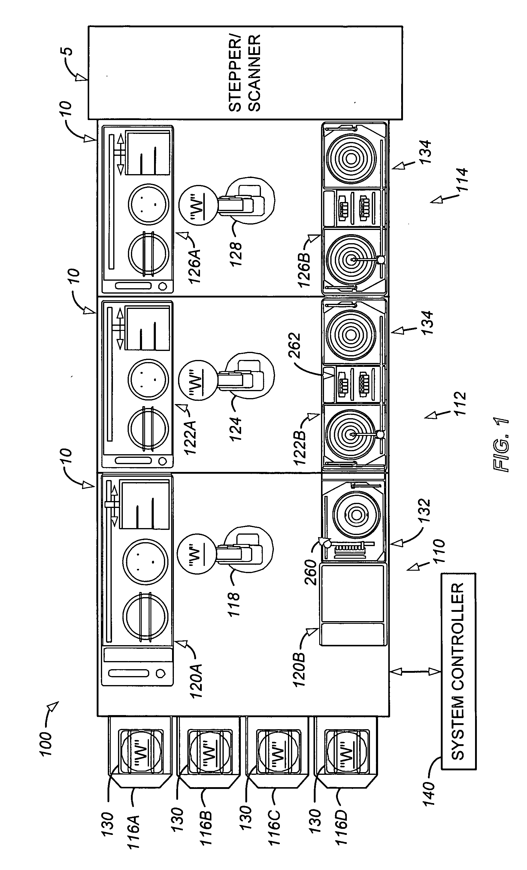
[0036]FIG. 1 is a plan view of an embodiment of a track lithography tool 100 in which the embodiments of the present invention may be used. As illustrated in FIG. 1, track lithography tool 100 contains a front end module 110 (sometimes referred to as a factory interface), a central module 112, and a rear module 114 (sometimes referred to as a scanner interface). Front end module 110 generally contains one or more pod assemblies or FOUPS (e.g., items 116A-D), a front end robot 118, and front end processing racks 120A and...


PUM


Abstract

Temperature of a processed workpiece may be regulated by flowing a thermal control fluid from a thermal source to a thermal drain, in a direction substantially normal to the plane occupied by the workpiece. This flow orientation ensures that any resulting temperature gradient in the thermal control fluid is also positioned substantially normal to the substrate, thereby avoiding processing variation in different areas of the workpiece attributable to an in-plane gradient. The thermal control fluid may be flowed from a common source to a plurality of pixel-like regions proximate to the workpiece, in order to ensure uniform temperature control. Use of such pixel-like regions promotes scalability of the temperature control apparatus.

Description

CROSS-REFERENCE TO RELATED APPLICATIONS [0001] This instant nonprovisional application is related to commonly assigned U.S. patent application 60 / 696,392, filed on Jul. 1, 2005, the entire disclosure of which is incorporated herein by reference.BACKGROUND OF THE INVENTION [0002] The present invention relates generally to the field of substrate processing equipment. More particularly, the present invention relates to a method and apparatus for controlling temperature of a semiconductor workpiece during processing. [0003] Semiconductor device geometries have dramatically decreased in size since such devices were first introduced several decades ago. As device geometries have become more dense, reductions in the spacing between device elements has occurred. The minimum linewidths achieved using semiconductor lithography systems, sometimes referred to as a critical dimension (CD), have decreased over time. [0004] Lithography or photolithography generally refers to processes for transfer...

Claims


Application Information

Patent Timeline
Patent Type & Authority Applications(United States)
IPC IPC(8): B05C11/00
CPCG03F7/707H01L21/67109G03F7/70875
Inventor LUE, BRIAN C.
Owner SOKUDO CO LTD
Why Eureka
Try Eureka