Gate electrode with double diffusion barrier and fabrication method of semiconductor device including the same

Inactive Publication Date: 2007-01-04
SK HYNIX INC
View PDF6 Cites 22 Cited by
  • Summary
  • Abstract
  • Description
  • Claims
  • Application Information

AI Technical Summary

Benefits of technology

[0016] It is, therefore, an object of the present invention to provide a gate electrode of a semiconductor device and a method for fabricating the same provided with a double diffusion barrier capable of inhibiting an insulation layer formation o

Problems solved by technology

However, there is a disadvantage.
Such insulation layer affects device operation characteristics such as a resistance capacitance (RC) delay.
Especially, such insulation layer induces faulty operations during a high-speed operation at high-frequency.
However, even when using the above-described double diffusion barrier, there arise limitations as shown in FIGS. 2A to 2C.
As shown in FIG. 2A, even in the case of an a-WNx/WSix double diffusion barrier, there exists a disadvantage of S—-N being formed on an interface between the tungsten layer and the polysilicon layer due to the reaction between silicon existing in WSiX and nitrogen decomposed from a-WNx.
Furthermore, as shown in FIG. 2B, in the case of an a-WNx/W double diffusion barrier, the a-WNx/W double diffusion barrier has extremely vulnerable heat s

Method used


Image

  • Gate electrode with double diffusion barrier and fabrication method of semiconductor device including the same
  • Gate electrode with double diffusion barrier and fabrication method of semiconductor device including the same
  • Gate electrode with double diffusion barrier and fabrication method of semiconductor device including the same

Examples


Embodiment Construction

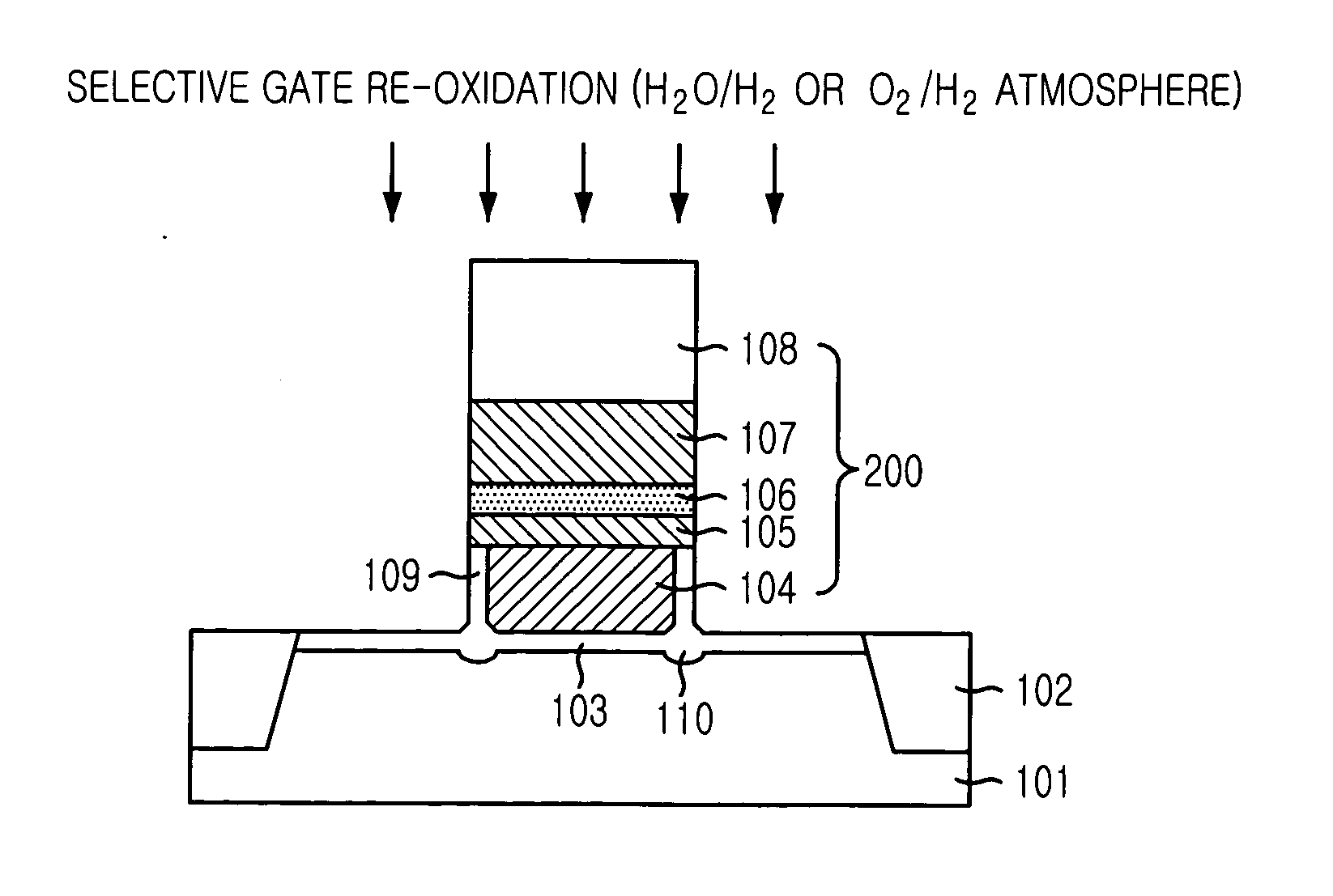
[0028] A gate electrode with a double diffusion barrier and a fabrication method of a semiconductor device including the same in accordance with exemplary embodiments of the present invention will be described in detail with reference to the accompanying drawings.

[0029]FIG. 3 is a cross-sectional view illustrating a poly-metal gate electrode structure in accordance with a specific embodiment of the present invention.

[0030] As shown in FIG. 3, the poly-metal gate electrode includes: a silicon electrode 31; a first diffusion barrier 32 formed on the silicon electrode 31; a second diffusion barrier 33 formed on the first diffusion barrier 32; and a metal electrode 34 formed on the second diffusion barrier 33. That is, the diffusion barrier of the poly-metal gate electrode has a double diffusion barrier structure including the first diffusion barrier 32 and the second diffusion barrier 33.

[0031] Firstly, the silicon electrode 31 is formed by employing one of polysilicon, polysilicon ...


PUM


Abstract

A gate electrode with a double diffusion barrier and a fabrication method of a semiconductor device including the same are provided. The gate electrode of a semiconductor device includes: a silicon electrode; a double diffusion barrier formed on the silicon electrode and including at least a crystalline tungsten nitride-based layer; and a metal electrode formed on the double diffusion barrier.

Description

FIELD OF THE INVENTION [0001] The present invention relates to a semiconductor device and a method for fabricating the same; and, more particularly, to a gate electrode in a semiconductor device with a double diffusion barrier and a method for fabricating a semiconductor device including the same. DESCRIPTION OF RELATED ARTS [0002] Recently, to reduce resistance of a gate electrode in a formation process of a semiconductor device, a polycide gate electrode with a tungsten silicide (WSix) / polysilicon structure and a tungsten poly-metal gate electrode with a tungsten (W) / tungsten nitride-based layer (WNx) / polysilicon structure, which further reduces resistance, are used. The tungsten nitride layer, which is used as a diffusion barrier in the tungsten poly-metal gate electrode, is in an amorphous state. The amorphous tungsten nitride layer is expressed as ‘a-WNx’, where x representing an atomic ratio of nitrogen ranges from 0.1 to 1.0. [0003]FIG. 1 is a cross-sectional view illustratin...

Claims


Application Information

Patent Timeline
IPC IPC(8): H01L29/94H01L21/3205
CPCH01L21/28061H01L29/78H01L29/4933H01L21/18
Inventor LIM, KWAN-YONGSUNG, MIN-GYUCHO, HEUNG-JAEYANG, HONG-SEONLEE, SEUNG-RYONG
Owner SK HYNIX INC
Why Eureka
Try Eureka